Do you have a question about the Clevo N150ZU and is the answer not in the manual?
General information about system elements and specifications.
Detailed technical specifications of the notebook computer.
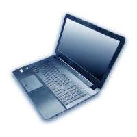
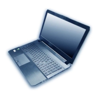
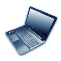
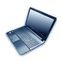
Locates components on the top of the notebook with the LCD open.
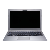
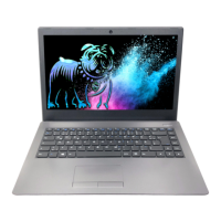
Identifies ports and features on the front and right side of the notebook.
Identifies ports and features on the left side and rear of the notebook.
Locates components on the bottom of the notebook.
Identifies key components on the top side of the mainboard.
Identifies key components on the bottom side of the mainboard.
Identifies connectors on the top side of the mainboard.
Identifies connectors on the bottom side of the mainboard.
Explains the step-by-step process for disassembling notebook parts and subsystems.
Lists recommended tools for performing maintenance on the notebook.
Describes four types of internal computer connections and how to release them.
Lists safety precautions to avoid personal injury or computer damage during repairs.
Provides instructions on how to clean the computer using a soft cloth.
Lists disassembly steps and corresponding page numbers for related information.
Provides detailed steps and illustrations for removing the keyboard module.
Details the procedure for removing the 36W battery from the notebook.
Details the procedure for removing the 54W battery from the notebook.
Explains how to remove the 2.5" SATA HDD or SSD from the notebook.
Provides steps for removing and installing SO-DIMM memory modules.
Details the procedure for removing the Wireless LAN module.
Describes identification and connection of antenna cables for WLAN/Bluetooth modules.
Provides steps for removing the M.2 SATA/PCIe SSD module.
Details the procedure for removing the CCD module and its front cover.
Table indicating where to find specific part list illustrations for notebook components.
Lists parts for the top case assembly with a fingerprint reader.
Lists parts for the top case assembly without a fingerprint reader.
Lists and illustrates parts for the bottom case assembly.
Lists and illustrates parts related to the LCD panel assembly.
Lists and illustrates parts for the mainboard assembly.
Illustrates the overall system architecture and component connections.
Detailed schematic for processor interfaces and memory signals (part 1 of 12).
Detailed schematic for processor interfaces and memory signals (part 2 of 12).
Detailed schematic for processor interfaces and memory signals (part 3 of 12).
Detailed schematic for processor interfaces and memory signals (part 4 of 12).
Detailed schematic for processor interfaces and memory signals (part 5 of 12).
Detailed schematic for processor interfaces and memory signals (part 6 of 12).
Detailed schematic for processor interfaces and memory signals (part 7 of 12).
Detailed schematic for processor interfaces and memory signals (part 8 of 12).
Detailed schematic for processor interfaces and memory signals (part 9 of 12).
Detailed schematic for processor interfaces and memory signals (part 10 of 12).
Detailed schematic for processor interfaces and memory signals (part 11 of 12).
Detailed schematic for processor interfaces and memory signals (part 12 of 12).
Circuit diagram for the DDR4 SO-DIMM slot A.
Circuit diagram for the DDR4 SO-DIMM slot B.
Circuit diagram for the HDMI connector.
Circuit diagram for the eDP panel connector and backlight.
Circuit diagram for the PS8338B chip, used for signal multiplexing.
Circuit diagram for the Mini DisplayPort connector.
Circuit diagram related to Thunderbolt (TBT) functionality.
Circuit diagram for power regulation related to Thunderbolt.
Circuit diagram for ASM1543 USB-C controller and redriver.
Circuit diagram for the TPS65987D USB Type-C power delivery controller.
Circuit diagram for the card reader and Ethernet LAN controller.
Circuit diagram for the ALC293D audio codec.
Circuit diagram for the ITE IT8587 keyboard controller.
Circuit diagram related to E/B Keys and WLAN/Bluetooth connections.
Circuit diagram for M.2 PCIE SSD slot and RTD3 power.
Circuit diagram for SATA interface, LEDs, and TPM module.
Circuit diagram for USB 3.1 port and charger functionality.
Circuit diagram for various connectors, CCD, fan, touchpad, and keyboard LEDs.
Circuit diagrams for 3V, 5V, 3VS, 5VS, 1.8VS power rails.
Circuit diagrams for VDD3 and VDD5 power rails.
Circuit diagrams for 1.05VA, VCCST, and VCCSTG power rails.
Circuit diagrams for VDDQ, VDDQ_VTT, 1.5VS, and 1.8VA power rails.
Circuit diagram for the AC adapter input and EMI check.
Circuit diagram for the VCore NCP81218 voltage regulator.
Circuit diagrams for VCCIN, VCCGT, and VCCSA power outputs.
Circuit diagrams for VCCIO and 2.5V power rails.
Circuit diagram for the smart charger and AC input.
Circuit diagram for the USB board, including USB 2.0 port.
Circuit diagram for the USB 3.1 Port 4, including redriver.
Circuit diagram for the audio board, including headphone and microphone jacks.
Circuit diagram for the touchpad click board.
Circuit diagram for the power, battery, and HDD LEDs.
Circuit diagram for the power switch and lid switch IC.
Instructions on how to download BIOS update files from the website.
Steps to unzip BIOS files onto a bootable CD/DVD/USB drive.
Instructions to configure the BIOS to boot from external media.
Guidance on selecting the correct BIOS version and compatibility notes.
Commands and steps to perform the BIOS update using flash tools.
Procedures for restarting the computer and loading default BIOS settings.