TABLE OF CONTENTS
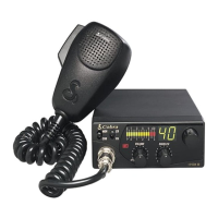
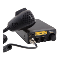
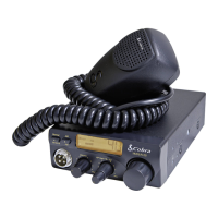
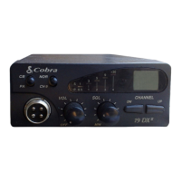
Model 19 Plus
DESCRIPTION PAGE NUMBER
OPERATING THEORY- PLL FREQ. SYNTHESIZER....................................................................1-4
FREQUENCY CHART (TABLE 1).......................................................................................
.
..................5
BLOCK DIAGRAM..................................................................................................................................... 6
PLL CIRCUIT BLOCK DIAGRAM
.............................
.
............................................................................7
ALIGNMENT PROCEDURE
................
8-11
TEST EQUIPMENT SET-UP
................................................
12
VOLTAGE CHART, IC’S & TRANSISTORS...................................................
.....................................
13
PARTS LAYOUT, PCB401068-F, TOP VIEW.......................................................................................14
COMPOSITE LAYOUT, PCB401068-F, TOP VIEW...............................
.
.........................................
14
COMPOSITE LAYOUT, PCB 401377-C, 401261-B, TOP VIEW
........................................................
14
PARTS LAYOUT, PCB401068-F, BOTTOM VIEW
...........
..
.................................................................15
PARTS LAYOUT, PCB 401377-C, 401261-B, BOTTOM VIEW............................................................15
COMPOSITE LAYOUT, PCB401068-F, BOTTOM VIEW.....................................................................16
COMPOSITE LAYOUT, PCB 401377-C, 401261-B, BOTTOM VIEW...................................................16
COPPER PATTERN, PCB401068-F, BOTTOM VIEW.........................................................................17
COPPER PATTERN, PCB 401377-C, 401261-B, BOTTOM VIEW.......................................................17
WIRING DIAGRAM, CHASSIS & MIC PINS..........................................................................................18
PCB 401068-D WIRING DIAGRAM.........................................................................................................19
SEMICONDUCTOR PIN CONFIGURATION..........................................................................................20
I.C. DIAGRAMS, LM6416E, LC7131, TA7310P.....................................................................................21
I.C. DIAGRAMS, KIA7217AP, TL489CP, MC78L08CT
...........................................................................
22
EXPLODED VIEW PARTS LIST.............................................................................................................23
EXPLODED VIEW
................................................
24
SCHEMATIC DIAGRAM..................................................................................................... 25
PARTS LIST........................................................ 25