These registers control the horizontal timing of the beginning and
end of the Bit Plane DMA display data fetch. The vertical Bit Plane
DMA
timing is identical to the Display windows described above. The
Bit
Plane Modulos are dependent on the Bit Plane horizontal size,
and on
this
data fetch window size.
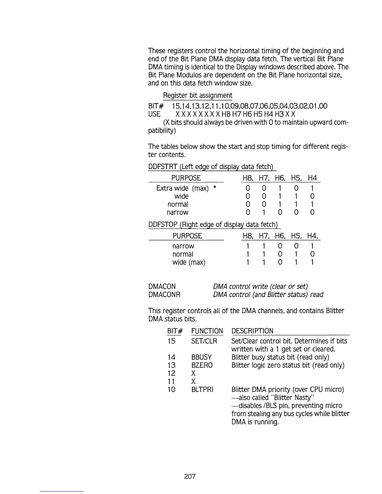
Register bit assignment
BIT#
1
5,14,13,12,11 ,l
0,09.08,07,06,05,04,03,02,01.00
USE
XXXXXXXXHBH7H6H5H4H3XX
(X
bits should always be driven with
0
to maintain upward com-
patibility)
The tables below show the start and stop timing for different regis-
ter contents.
DDFSTRT (Left edge of display data fetch)
PURPOSE
H8,
H7, H6. H5, H4
Extra wide (max)
*
00101
wide
00110
normal
00111
narrow
01000
DDFSTOP (Right edge of display data fetch)
PURPOSE
H8,
H7, H6, H5, H4,
narrow
11001
normal
11010
wide (max)
11011
DMACON
DMA
control write (clear or set)
DMACONR
DMA
control (and Blitter status) read
This register controls all of the DMA channels, and contains Biitter
DMA status bits.
BIT# FUNCTION DESCRIPTION
15
SETICLR SetIClear control bit. Determines if bits
written with a
1
get set or cleared.
14
BBUSY Blitter busy status bit (read only)
13
BZERO Blitter logic zero status bit (read only)
12
X
11
X
10
BLTPRl Blitter DMA priority (over CPU micro)
-also called "Blitter Nasty"
-disables
IBLS pin, preventing micro
from stealing any bus cycles while blitter
DMA
is
running.