43
1
1
KEY
t/110
14
15
16
17
’
CD3
CD2
GDI CDO
_|
HOLD 0
0 0
0 1
)
RATIO
0
0 0
1
1
1
TEST
0
0 1
0
,
SPEC
0
0
1
1
i
1
(A-B)
0
1 0 0
!
dB
0
1
0
1
0
1 1
0
1
1
MAX 0
1
1 1
i
1
MIN
1 0
0 0
!
;
RESET
1
0
0
1
!
1
MAN 1 0
1 0
INPUT
1
FILTER 1
1 0
1 1
AC
1 1
1
1
1
M7
KEY
14 15 16
17
1
CD7
CD6
CD5
CD4
:
100
0 0
0
0
10 0 0
0
1
1000 0
0
1 0
10MI7
0
0
1
1
1 0
1
0 0
.1 0 1
0
1
10S2 0
1
1 0
AUTO
0
1 1
1
i
DC
1 0
0 0
kL2
1 0 0
1
!
KEYBOARD
1
1
0 1
1
1
1 1
1
0
!
INPUT
ZERO
1
1 1 1
FIG. 3.45 CMOS
DATA BUS
: KEY SELECT
CODING
J
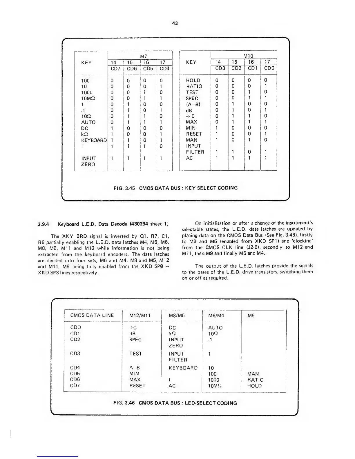
3.9.4 Keyboard L.E.D.
Data
Decode (430294
sheet
1)
The
XKY
BRD
signal is inverted by
Q1,
R7, Cl,
R6
partially enabling the L.E.D. data latches M4, M5,
M6,
M8,
M9, Mil
and
M12
while information is not being
extracted from the keyboard
encoders. The data
latches
are divided into four sets, M6 and M4,
M8
and
M5,
Ml
2
and Mil,
M9
being fully enabled from
the XKD SP0
—
XKD SP3 lines respectively.
On
initialisation or
after
a
change of the
instrument's
selectable states, the
L.E.D. data
latches are
updated by
placing data
on the CMOS
Data Bus
(See
Fig.
3.46),
firstly
to
M8 and M5
(enabled
from XKD
SP1)
and
'clocking'
from
the
CMOS
CLK
line (J2-6),
secondly to M12
and
Mil,
then
M9
and finally M6
and M4.
The
output
of the
L.E.D.
latches provide the
signals
to
the bases
of the L.E.D.
drive
transistors, switching
them
on or
off
as
required.
CMOS DATA LINE
M12/M11 M8/M5 M6/M4 M9
CDO
-^C DC AUTO
CD1
dB
k£2
1012
CD2
SPEC INPUT
ZERO
1
CD3 TEST
INPUT
FILTER
1
1
CD4 A-B
KEYBOARD 10
CD5
MIN
100
MAN
CD6
MAX
1
1000 RATIO
CD7
RESET
AC 10MI2 HOLD
FIG.
3.46
CMOS DATA BUS
; LED-SELECT
CODING
J
 Loading...