46
3.11 IEEE 488 STANDARD DIGITAL
INTERFACE
(Circuit Diagram
No. 430427)
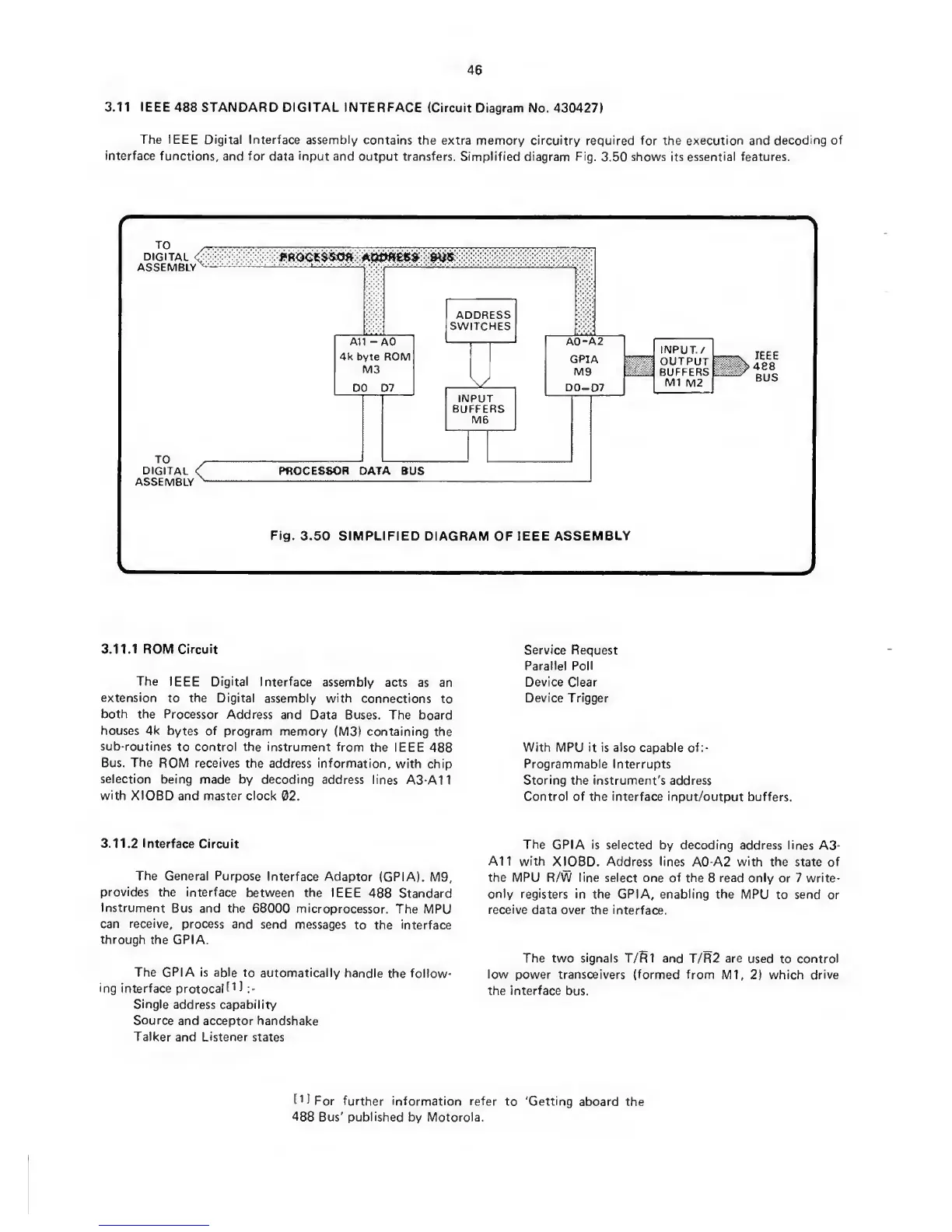
The IEEE Digital Interface assembly
contains
the extra memory circuitry required
for
the execution and decoding
of
interface
functions, and for
data input and
output
transfers.
Simplified diagram Fig.
3.50
shows its
essential features.
IEEE
488
BUS
Fig.
3.50 SIMPLIFIED
DIAGRAM
OF
IEEE
ASSEMBLY
3.11.1
ROM Circuit
The
IEEE Digital Interface
assembly
acts
as an
extension
to the
Digital
assembly with
connections
to
both the
Processor
Address and
Data Buses. The board
houses
4k bytes of
program memory
(M3) containing
the
sub-routines
to control the instrument
from
the IEEE
488
Bus. The
ROM
receives
the
address information,
with chip
selection being
made by decoding
address lines
A3-A11
with
XIOBD
and master clock
02.
3.11.2
interface Circuit
The General
Purpose
Interface Adaptor
(GPIA).
M9,
provides
the interface
between the
IEEE
488 Standard
Instrument
Bus and
the 68000
microprocessor.
The MPU
can receive,
process
and send messages
to the interface
through the GPIA.
The GPIA is
able to automatically
handle
the follow-
ing interface
protocalC*)
;•
Single
address
capability
Source
and
acceptor
handshake
Talker and Listener
states
Service Request
Parallel Poll
Device Clear
Device Trigger
With MPU it is also capable of;-
Programmable
Interrupts
Storing
the instrument's address
Control of
the interface input/output buffers.
The
GPIA is selected
by decoding address lines
A3-
A11 with
XIOBD. Address lines
A0-A2
with
the state of
the MPU R/W line
select
one
of the
8
read only or 7
write-
only
registers in the GPIA, enabling
the MPU
to
send or
receive
data over the
interface.
The two signals T/Rl and
T/R2
are
used
to
control
low power transceivers
(formed from Ml,
2)
which
drive
the interface
bus.
(I
I
For further information refer
to
'Getting
aboard
the
488
Bus'
published
by Motorola.
 Loading...