47
50 WAY
'CONNECTOR
24 WAY
'CONNECTOR
PROCESSOR DATA
BUS
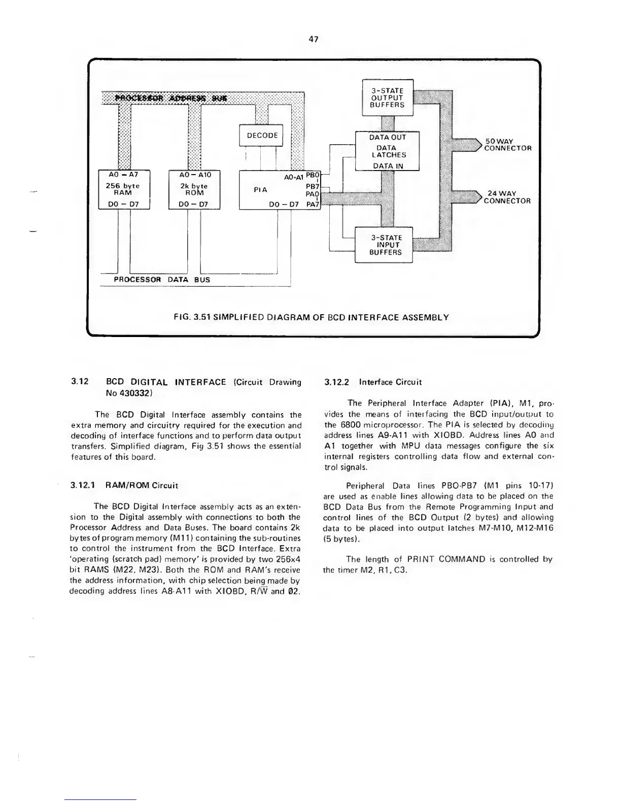
FIG.
3.51 SIMPLIFIED
DIAGRAM
OF
BCD
INTERFACE ASSEMBLY
3.12
BCD
DIGITAL
INTERFACE
(Circuit
Drawing
No 430332)
The
BCD
Digital
Interface assembly contains the
extra memory and
circuitry required
for
the execution and
decoding of interface functions and to
perform
data
output
transfers.
Simplified
diagram.
Fig 3.51 shows the essential
features of this
board.
3.12.1 RAM/ROM
Circuit
The
BCD
Digital
Interface assembly acts as an exten-
sion
to
the Digital
assembly
with
connections
to
both the
Processor
Address
and Data Buses.
The board contains 2k
bytes of program
memory
(Mil) containing
the sub-routines
to
control the instrument from
the BCD Interface.
Extra
'operating (scratch pad)
memory' is provided
by two 256x4
bit RAMS
(M22, M23). Both
the
ROM and
RAM's
receive
the address information, with chip
selection being
made by
decoding address lines
A8 A11
with
XIOBD, R/W and
02.
3.12.2
Interface Circuit
The
Peripheral Interface Adapter (PI
A),
Ml, pro
vides the means of
interfacing the
BCD input/output to
the 6800
microprocessor. The
PI
A
is
selected
by
decoding
address lines A9-A11 with XIOBD. Address lines AO and
A1
together with MPU
data
messages
configure the six
internal registers controlling data
flow and external con-
trol signals.
Peripheral Data lines
PBO-PB7 (Ml pins
10-17)
are used as
enable lines
allowing data to be
placed
on
the
BCD Data Bus
from the Remote
Programming Input and
control lines
of
the BCD
Output
(2
bytes)
and allowing
data to
be placed
into output latches M7-M10, Ml 2-MI 6
(5
bytes).
The length
of PRINT COMMAND is controlled
by
the timer M2, R1,
C3.
 Loading...