- 5 -
CR# Attrib. Register name Explanation
#115 O R/W Output update time of CH2
range:K0~K100. Default =H’0000.
#116 O R/W Output update time of CH3
#117 O R/W Output update time of CH4
#118 O R/W LV output mode setting
Set the output mode of CH1~CH4 when the
power is at LV (low voltage) condition.
Default= H’0000.
Symbols:
O: When CR#41 is set to H’5678, the set value of CR will be saved.
X: set value will not be saved.
R: able to read data by using FROM instruction.
W: able to write data by using TO instruction.
※ CR#43: Error status value. See the table below:
Description
bit0 K1 (H’1) Power supply error bit11 K2048(H’0800)
Upper / lower bound
setting error
bit1 K2 (H’2) Reserved bit12 K4096(H’1000)
Set value changing
prohibited
bit2 K4 (H’4)
Upper / lower
bound error
bit13 K8192(H’2000)
Communication
breakdown on next
module
bit9 K512(H’0200) Mode setting error
Note: Each error status is determined by the corresponding bit (b0 ~ b13) and there may be more
than 2 errors occurring at the same time. 0 = normal; 1 = error
※ Module Reset (available for firmware V1.12 or above): When modules need reset, write
H’4352 to CR#0, then wait for one second and then power off and restart. The instruction
initializes all parameter setups. To avoid the resetting process affecting the normal operation
of other modules, it is recommended to connect only one module at a time.
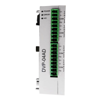
Explanation on Special Registers D9900~D9999
When DVP-ES2 MPU is connected with modules, registers D9900~D9999 will be
reserved for storing values from modules. You can apply MOV instruction to operate
values in D9900~D9999.
When ES2 MPU is connected with DVP02DA-E2/DVP04DA-E2, the configuration of
special registers is as below:
Module
#0
Module
#1
Module
#2
Module
#3
Module
#4
Module
#5
Module
#6
Module
#7
Description
D1320 D1321 D1322 D1323 D1324 D1325 D1326 D1327 Model Code
D9900 D9910 D9920 D9930 D9940 D9950 D9960 D9970 CH1 output value
D9901 D9911 D9921 D9931 D9941 D9951 D9961 D9971 CH2 output value
D9902 D9912 D9922 D9932 D9942 D9952 D9962 D9972 CH3 output value
D9903 D9913 D9923 D9933 D9943 D9953 D9963 D9973 CH4 output value
Adjust D/A Conversion Curve
Users can adjust the conversion curves according to the actual needs by changing the
Offset value (CR#28 ~ CR#31) and Gain value (CR#34 ~ CR#37).
Gain: The corresponding voltage/current input value when the digital output value =
16,000.
Offset: The corresponding voltage/current input value when the digital output value = 0.
Equation for voltage output Mode0: 0.3125mV = 20V/64,000
 Loading...