DIGITAL_OSD : IC732
EN25QH32B104HIP2B (except : E2)
EN25QH64A104HIP (ONLY E2)
SN74CBT3251PWR (DIGITAL_OSD : IC733)
Block diagram
8 - LEAD SOP / PDIP
DO (DQ
1
)
WP# (DQ
2
)
VSS
CS#
DI (DQ
0
)
CLK
HOLD# (DQ
3
)
VCC
Table 1. Pin Names
Symbol Pin Name
CLK Serial Clock Input
DI (DQ
0
) Serial Data Input (Data Input Output 0)
*1
DO (DQ
1
) Serial Data Output (Data Input Output 1)
*1
CS# Chip Select
WP# (DQ
2
) Write Protect (Data Input Output 2)
*2
HOLD# (DQ
3
) HOLD# pin (Data Input Output 3)
*2
Vcc Supply Voltage (2.7-3.6V)
Vss Ground
NC No Connect
Note:
1. DQ
0
and DQ
1
are used for Dual and Quad instructions.
2. DQ
2
~ DQ
3
are used for Quad instructions.
SN74CBT3251
1-OF-8 FET MULTIPLEXER/DEMULTIPLEXER
SCDS019L − MAY 1995 − REVISED JANUARY 2004
1
POST OFFICE BOX 655303 • DALLAS, TEXAS 75265
5-Ω Switch Connection Between Two Ports TTL-Compatible Input Levels
1
2
3
4
5
6
7
8
16
15
14
13
12
11
10
9
B4
B3
B2
B1
A
NC
OE
GND
V
CC
B5
B6
B7
B8
S0
S1
S2
D, DB, DBQ, OR PW PACKAGE
(TOP VIEW)
NC − No internal connection
RGY PACKAGE
(TOP VIEW)
1 16
89
2
3
4
5
6
7
15
14
13
12
11
10
B5
B6
B7
B8
S0
S1
B3
B2
B1
A
NC
OE
B4
S2
V
GND
CC
NC − No internal connection
description/ordering information
The SN74CBT3251 is a 1-of-8 high-speed TTL-compatible FET multiplexer/demultiplexer. The low on-state
resistance of the switch allows connections to be made with minimal propagation delay.
When output enable (OE
) is low, the SN74CBT3251 is enabled. S0, S1, and S2 select one of the B outputs for
the A-input data.
ORDERING INFORMATION
T
A
PACKAGE
†
ORDERABLE
PART NUMBER
TOP-SIDE
MARKING
QFN − RGY Tape and reel SN74CBT3251RGYR CU251
SOIC − D
Tape and reel SN74CBT3251DR
CBT3251
−40°C to 85°C
SSOP − DB Tape and reel SN74CBT3251DBR CU251
SSOP (QSOP) − DBQ Tape and reel SN74CBT3251DBQR CU251
TSSOP − PW
Tape and reel SN74CBT3251PWR
CU251
†
Package drawings, standard packing quantities, thermal data, symbolization, and PCB design
guidelines are available at www.ti.com/sc/package.
Copyright © 2004, Texas Instruments Incorporated
PRODUCTION DATA information is current as of publication date.
Products conform to specifications per the terms of Texas Instruments
standard warranty. Production processing does not necessarily include
testing of all parameters.
Please be aware that an important notice concerning availability, standard warranty, and use in critical applications of
Texas Instruments semiconductor products and disclaimers thereto appears at the end of this data sheet.
SN74CBT3251
1-OF-8 FET MULTIPLEXER/DEMULTIPLEXER
SCDS019L − MAY 1995 − REVISED JANUARY 2004
2
POST OFFICE BOX 655303 • DALLAS, TEXAS 75265
FUNCTION TABLE
(each multiplexer/demultiplexer)
INPUTS
OE S2 S1 S0
FUNCTION
L L L L A port = B1 port
L L L H A port = B2 port
L L H L A port = B3 port
L L H H A port = B4 port
L H L L A port = B5 port
L H L H A port = B6 port
L H H L A port = B7 port
L H H H A port = B8 port
H X X X Disconnect
logic diagram (positive logic)
B5
B1
A
B2
B3
B4
B6
B7
B8
OE
S0
S1
S2
5
7
11
10
9
4
3
2
1
15
14
13
12
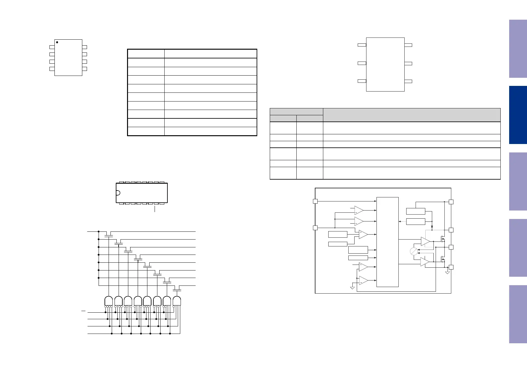
TPS563200 (DIGITAL_DIGITAL SUPPLY : IC741, IC742, IC743, IC744)
Terminal Functions
PIN
DESCRIPTION
NAME NUMBER
GND 1
Ground pin Source terminal of low-side power NFET as well as the ground ter-
minal for controller circuit. Connect sensitive VFB to this GND at a single point.
SW 2 Switch node connection between high-side NFET and low-side NFET.
VIN 3 Input voltage supply pin. The drain terminal of high-side power NFET.
VFB 4
Converter feedback input. Connect to output voltage with feedback resistor
divider.
EN 5 Enable input control. Active high and must be pulled up to enable the device.
VBST 6
Supply input for the high-side NFET gate drive circuit. Connect a 0.1 μ F ca-
pacitor between VBST and SW pins.
Block diagram
SW
VBST
VFB
GND
2
3
1
EN
4
6
5
VIN
TPS562200, TPS563200
DDC (SOT) Package
Top View
2 SW
ZC
XCON
PWM
Control Logic
+
+
+
UVP
OVP
3 VIN
Ton
One-Shot
6
VBST
+
4
VFB
OCL
+
+
Soft Start
5EN
HS
LS
1 GND
SS
Voltage
Reference
Ref
Hiccup
V
UVP
V
OVP
OCL
threshold
Regulator
UVLO
VREG5
VREG5
TSD
Before Servicing
This Unit
Electrical Mechanical Repair Information Updating
47
 Loading...