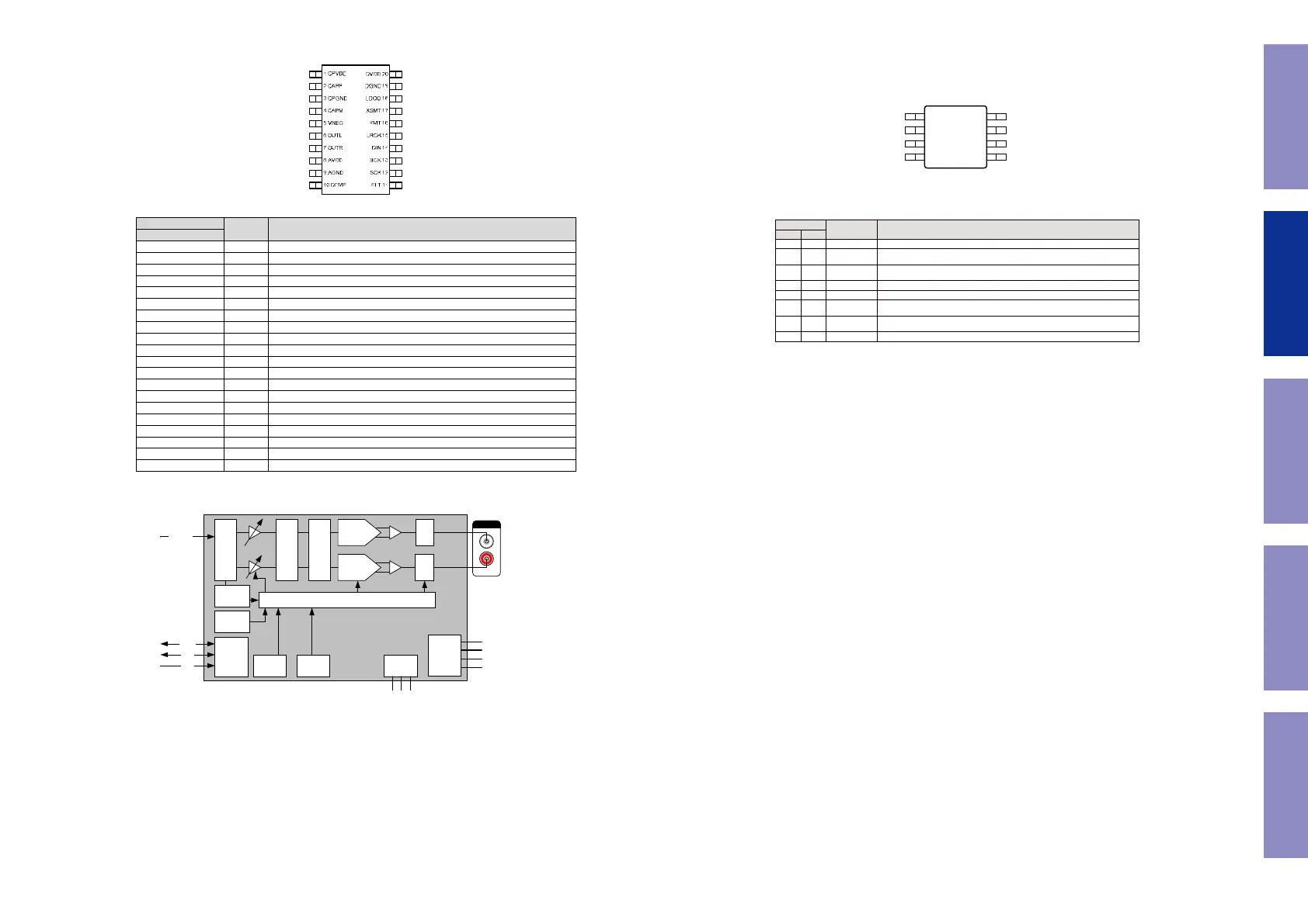
PCM5100APWR (DIGITAL_NETWORK : IC760, IC765)
Block diagram
Pin Functions
PIN
TYPE DESCRIPTION
NAME NO.
AGND 9 — Analog ground
AVDD 8 P Analog power supply, 3.3 V
BCK 13 I Audio data bit clock input
(1)
CAPM 4 O Charge pump flying capacitor terminal for negative rail
CAPP 2 O Charge pump flying capacitor terminal for positive rail
CPGND 3 — Charge pump ground
CPVDD 1 P Charge pump power supply, 3.3 V
DEMP 10 I De-emphasis control for 44.1-kHz sampling rate
(1)
: Off (Low) / On (High)
DGND 19 — Digital ground
DIN 14 I Audio data input
(1)
DVDD 20 P Digital power supply, 1.8 V or 3.3 V
FLT 11 I Filter select : Normal latency (Low) / Low latency (High)
FMT 16 I Audio format selection : I
2
S (Low) / Left-justified (High)
LDOO 18 P Internal logic supply rail terminal for decoupling, or external 1.8 V supply terminal
LRCK 15 I Audio data word clock input
(1)
OUTL 6 O Analog output from DAC left channel
OUTR 7 O Analog output from DAC right channel
SCK 12 I System clock input
(1)
VNEG 5 O Negative charge pump rail terminal for decoupling, –3.3 V
XSMT 17 I Soft mute control
(1)
: Soft mute (Low) / soft un-mute (High)
(1) Failsafe LVCMOS Schmitt trigger input
Audio Interface
8x Interpolation Filter
32bit Modulator
Current
Segment
DAC
Current
Segment
DAC
I/V I/V
Analog
Mute
Analog
Mute
Zero
Data
Detector
UVP/Reset
PLL Clock
Power
Supply
Ch. PumpPOR
Clock Halt
Detection
Advanced Mute Control
SCK
BCK
LRCK
CAPP
LINE OUT
DIN (i2s)
PCM510xA
CPVDD (3.3V)
AVDD (3.3V)
GND
TCA9517DGKR (F-HDMI : IC311)
Terminal Functions
1
8
VCCA VCCB
4
5
GND EN
3 6
SDAA SDAB
2
7
SCLA SCLB
DGK Package
8-Pin VSSOP
Top View
PIN
TYPE DESCRIPTION
NO. NAME
1 VCCA Supply A-side supply voltage (0.9 V to 5.5 V)
2 SCLA Input/Output
Serial clock bus, A-side. Connect to V
CCA
through a pull-up resistor. If unused, connect directly to
ground.
3 SDAA Input/Output
Serial data bus, A-side. Connect to V
CCA
through a pull-up resistor. If unused, connect directly to
ground.
4 GND Ground Ground
5 EN Input Active-high repeater enable input
6 SDAB Input/Output
Serial data bus, B-side. Connect to V
CCB
through a pull-up resistor. If unused, connect directly to
ground.
7 SCLB In p ut /O u tp ut
Serial clock bus, B-side. Connect to V
CCB
through a pull-up resistor. If unused, connect directly to
ground.
8 VCCB Supply B-side and device supply voltage (2.7 V to 5.5 V)
Before Servicing
This Unit
Electrical Mechanical Repair Information Updating
56
 Loading...