ADV7623 Hardware Manual
Rev. 0 – March 2010 22 Confidential NDA required
Location Mnemonic Type Description
111 CGND Ground TVDD and CVDD Ground
112 RXA_C- HDMI Input Digital input clock Complement of port A
in the HDMI interface.
113 RXA_C+ HDMI Input Digital input clock True of port A in the
HDMI interface.
114 TVDD Power Receiver terminator supply voltage (3.3 V)
115 RXA_0- HDMI Input Digital input channel 0 complement of port
A in the HDMI interface.
116 RXA_0+ HDMI Input Digital input channel 0 true of port A in the
HDMI interface.
117 CGND Ground TVDD and CVDD Ground
118 RXA_1- HDMI Input Digital input channel 1 complement of port
A in the HDMI interface.
119 RXA_1+ HDMI Input Digital input channel 1 true of port A in the
HDMI interface.
120 TVDD Power Receiver terminator supply voltage (3.3 V)
121 RXA_2- HDMI Input Digital input channel 2 complement of port
A in the HDMI interface.
122 RXA_2+ HDMI Input Digital input channel 2 true of port A in the
HDMI interface.
123 HP_CTRLB Digital Output Hot Plug Detect for port B.
124 5V_DETB Digital Input 5 V detect pin for port B in the HDMI
interface.
125 DGND Ground Ground for DVDD
126 DVDD Power Digital supply voltage (1.8 V)
127 DDCB_SDA Digital I/O HDCP slave serial data ports B.
DDCB_SDA is a 3.3 V input/output that is
5 V tolerant.
128 DDCB_SCL Digital Input HDCP slave serial clock port B.
DDCB_SCL is a 3.3 V input that is 5 V
tolerant.
129 CVDD Power Receiver comparator supply voltage (1.8V)
130 CGND Ground TVDD and CVDD Ground
131 RXB_C- HDMI Input Digital input clock complement of port B in
the HDMI interface.
132 RXB_C+ HDMI Input Digital input clock true of port B in the
HDMI interface.
133 TVDD Power Receiver terminator supply voltage (3.3 V)
134 RXB_0- HDMI Input Digital input channel 0 complement of port
B in the HDMI interface.
135 RXB_0+ HDMI Input Digital input channel 0 true of port B in the
HDMI interface.
136 CGND Ground TVDD and CVDD Ground
137 RXB_1- HDMI Input Digital input channel 1 complement of port
EN25QH32B104HIP2B (DIGITAL : IC722, IC732)
ADV7623 Hardware Manual
Rev. 0 – March 2010 23 Confidential NDA required
Location Mnemonic Type Description
B in the HDMI interface.
138 RXB_1+ HDMI Input Digital input channel 1 true of port B in the
HDMI interface.
139 TVDD Power Receiver terminator supply voltage (3.3 V)
140 RXB_2- HDMI Input Digital input channel 2 complement of port
B in the HDMI interface.
141 RXB_2+ HDMI Input Digital input channel 2 true of port B in the
HDMI interface.
142 HP_CTRLC Digital Output Hot Plug Detect for port C.
143 5V_DETC Digital Input 5 V detect pin for port C in the HDMI
interface.
144 DDCC_SDA Digital I/O HDCP slave serial clock port C.
DDCC_SDA is a 3.3 V input/output that is
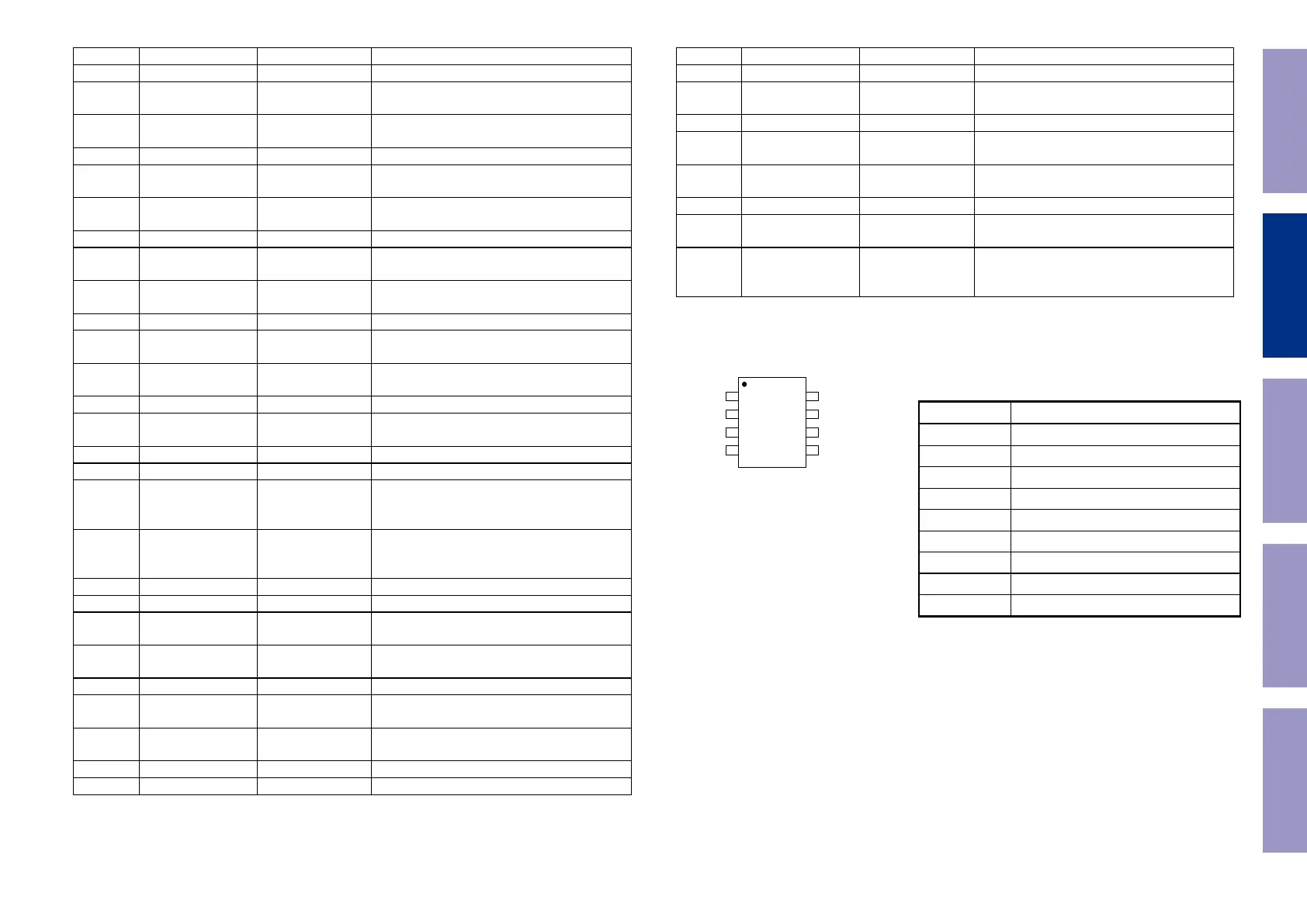
8 - LEAD SOP / PDIP
DO (DQ
1
)
WP# (DQ
2
)
VSS
CS#
DI (DQ
0
)
CLK
HOLD# (DQ
3
)
VCC
Table 1. Pin Names
Symbol Pin Name
CLK Serial Clock Input
DI (DQ
0
) Serial Data Input (Data Input Output 0)
*1
DO (DQ
1
) Serial Data Output (Data Input Output 1)
*1
CS# Chip Select
WP# (DQ
2
) Write Protect (Data Input Output 2)
*2
HOLD# (DQ
3
) HOLD# pin (Data Input Output 3)
*2
Vcc Supply Voltage (2.7-3.6V)
Vss Ground
NC No Connect
Note:
1. DQ
0
and DQ
1
are used for Dual and Quad instructions.
2. DQ
2
~ DQ
3
are used for Quad instructions.
Before Servicing
This Unit
Electrical Mechanical Repair Information Updating
39

 Loading...