PCM5100APWR (BT : IC901)
Block diagram
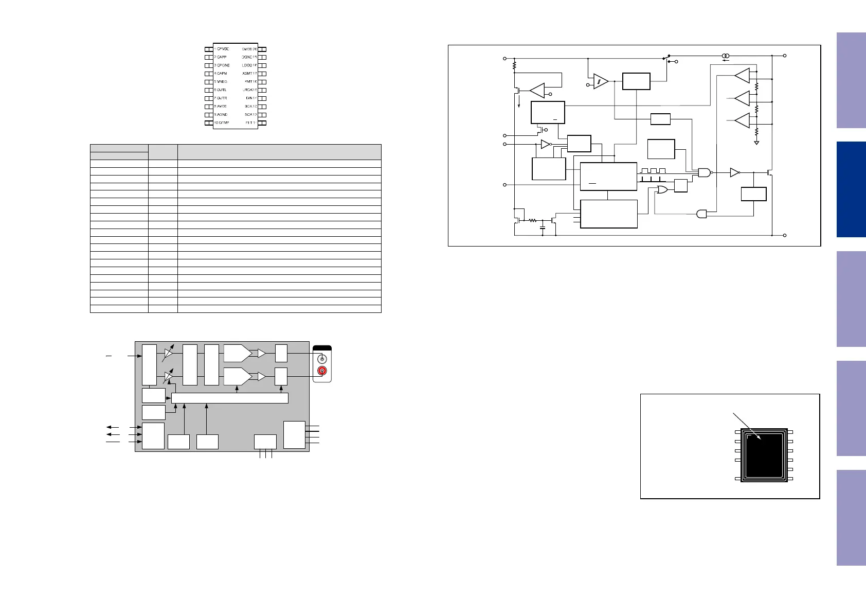
Pin Functions
PIN
TYPE DESCRIPTION
NAME NO.
AGND 9 — Analog ground
AVDD 8 P Analog power supply, 3.3 V
BCK 13 I Audio data bit clock input
(1)
CAPM 4 O Charge pump flying capacitor terminal for negative rail
CAPP 2 O Charge pump flying capacitor terminal for positive rail
CPGND 3 — Charge pump ground
CPVDD 1 P Charge pump power supply, 3.3 V
DEMP 10 I De-emphasis control for 44.1-kHz sampling rate
(1)
: Off (Low) / On (High)
DGND 19 — Digital ground
DIN 14 I Audio data input
(1)
DVDD 20 P Digital power supply, 1.8 V or 3.3 V
FLT 11 I Filter select : Normal latency (Low) / Low latency (High)
FMT 16 I Audio format selection : I
2
S (Low) / Left-justified (High)
LDOO 18 P Internal logic supply rail terminal for decoupling, or external 1.8 V supply terminal
LRCK 15 I Audio data word clock input
(1)
OUTL 6 O Analog output from DAC left channel
OUTR 7 O Analog output from DAC right channel
SCK 12 I System clock input
(1)
VNEG 5 O Negative charge pump rail terminal for decoupling, –3.3 V
XSMT 17 I Soft mute control
(1)
: Soft mute (Low) / soft un-mute (High)
(1) Failsafe LVCMOS Schmitt trigger input
Audio Interface
8x Interpolation Filter
32bit Modulator
Current
Segment
DAC
Current
Segment
DAC
I/V I/V
Analog
Mute
Analog
Mute
Zero
Data
Detector
UVP/Reset
PLL Clock
Power
Supply
Ch. PumpPOR
Clock Halt
Detection
Advanced Mute Control
SCK
BCK
LRCK
CAPP
LINE OUT
DIN (i2s)
PCM510xA
CPVDD (3.3V)
AVDD (3.3V)
GND
TOP268VG (SMPS : IC601)
Figure 3. Functional Block Diagram.
PI-4511-012810
SHUTDOWN/
AUTO-RESTART
CLOCK
CONTROLLED
TURN-ON
GATE DRIVER
CURRENT LIMIT
COMPARATOR
INTERNAL UV
COMPARATOR
INTERNAL
SUPPLY
5.8 V
4.8 V
SOURCE (S)
SOURCE (S)
S
R
Q
D
MAX
STOP
SOFT
START
CONTROL (C)
VOLTAGE
MONITOR (V)
FREQUENCY (F)
-
+
5.8 V
I
FB
1 V
Z
C
V
C
+
-
+
-
+
-
LEADING
EDGE
BLANKING
÷ 16
1
HYSTERETIC
THERMAL
SHUTDOWN
SHUNT REGULATOR/
ERROR AMPLIFIER
+
-
DRAIN (D)
ON/OFF
DC
MAX
DC
MAX
66k/132k
0
OV/
UV
OVPV
V
I (LIMIT)
CURRENT
LIMIT
ADJUST
V
BG
+ V
T
LINE
SENSE
SOFT START
OFF
F REDUCTION
F REDUCTION
STOP LOGIC
EXTERNAL CURRENT
LIMIT (X)
OSCILLATOR
WITH JITTER
PWM
K
PS(UPPER)
K
PS(LOWER)
SOFT START
I
FB
I
PS(UPPER)
I
PS(LOWER)
K
PS(UPPER)
K
PS(LOWER)
Pin Functional Description
DRAIN (D) Pin:
High-voltage power MOSFET DRAIN pin. The internal start-up
bias current is drawn from this pin through a switched high-
voltage current source. Internal current limit sense point for
drain current.
CONTROL (C) Pin:
Error amplifier and feedback current input pin for duty cycle
control. Internal shunt regulator connection to provide internal
bias current during normal operation. It is also used as the
connection point for the supply bypass and auto-restart/
compe
nsation capacitor.
EXTERNAL CURRENT LIMIT (X) Pin:
Input pin for external current limit adjustment remote-ON/OFF
and device reset. A connection to SOURCE pin disables all
functions on this pin. This pin should not be left floating.
VOLTAGE MONITOR (V) Pin:
Input for OV, UV, line feed-forward with DC
MAX
reduction, output
overvoltage protection (OVP), remote-ON/OFF. A connection to
the SOURCE pin disables all functions on this pin. This pin should
not be left flo
ating.
FREQUENCY (F) Pin :
Input pin for selecting switching frequency 132 kHz if connected
to SOURCE pin and 66 kHz if connected to CONTROL pin. This
pin should not be left floating.
SOURCE (S) Pin:
Output MOSFET source connection for high-voltage power return.
Primary-side control circuit common and reference point.
NO CONNECTION (NC) Pin:
Internally not connected, floating potential pin.
Figure 4. Pin Configuration (Top View).
12 S
11 S
10 S
9 S
8 S
7 S
V 1
X 2
C 3
F 4
D 6
PI-5568-061011
K Package
(eSOP-12B)
Exposed Pad (On Bottom)
Internally Connected to
SOURCE Pin
Before Servicing
This Unit
Electrical Mechanical Repair Information Updating
44

 Loading...