Advanced Function Instruction
7-60
FUN 79 D
7SGDL
7-SEGMENT OUTPUT WITH LATCH
FUN 79 D
7SGDL
S : Register storing the data (BCD) to be
displayed
OT : Starting number of scanning output
N : Specify signal output and polarity of latch
WR : Working register, it can't repeat in use
S may combine with V、Z、P0~P9 to serve
indirect addressing application
Y WX WY WM WS TMR CTR HR IR OR SR ROR DR K XR
Range
Ope-
rand
Y0
∣
Y240
WX0
∣
WX240
WY0
∣
WY240
WM0
∣
WM1896
WS0
∣
WS984
T0
∣
T255
C0
∣
C255
R0
∣
R3839
R3840
∣
R3903
R3904
∣
R3967
R3968
∣
R4167
R5000
∣
R8071
D0
∣
D4095
16-bit
number
V、Z
P0~P9
S ○ ○ ○ ○ ○ ○ ○ ○ ○ ○ ○ ○ ○
OT ○
N 0~3
z When input control "EN" = 1, the 4 nibbles of the S register, from digit 0 to digit 3, are sequentially sent out to
the 4 output points, OT0~OT3. While output the digit data, the latch signal of that digit (OT4 corresponds to
digit 0, OT5 corresponds to digit 1, etc...) at the same time is also sent out so that the digital value will be
loaded and latched into the 7-segment display respectively.
z When in D (32-bit) instruction, nibbles 0~3 from the S register, and nibbles 0~3 from the S+1 register are
transferred separately to OT0~OT3 and OT8~OT11. Because they are transferred at the same time, they can
use the same latch signal. 16-bit instructions do not use OT8~OT11.
z As long as "EN" remains 1, PLC will execute the transfer cyclically. After each transfer of a complete group of
numerical values (nibbles 0~3 or 0~7), the output completed flag "DN" will set to 1. However, it will only be kept
for 1 scan.
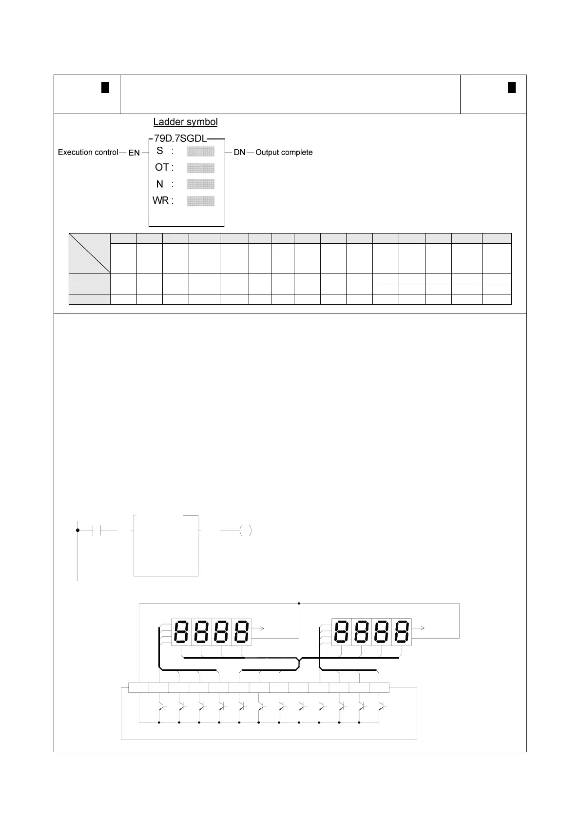
EN
DN
M10
OT :
Y0
WR : D0
X0
79D.7SGDL
N :
S :
R0
2
z In this example, when X0=1, the 4 nibbles of R0
will be transferred to the first group 7-segment
display in the diagram below. The 4 nibbles of R1
will be transferred to the second group 7-segment
display.
first group
second group
VCC
VCC
COM
COM
1
2
4
8
8
4
2
1
10
3
10
2
PLC transistor output
NPN
10
1
10
0
10
10 10 10
0
12
3
1
2
4
8
0
10
8
4
2
1
1
10
10
2
10
3
CY0Y1
Y2
Y3 Y4
Y5
Y6
Y7 Y8 Y9
Y10
Y11