Do you have a question about the Fibocom NL668-LA Series and is the answer not in the manual?
Overview of the NL668-LA hardware guide's content and purpose.
Essential safety guidelines for using the NL668-LA module to prevent hazards and damage.
Introduces the NL668-LA series module and its applicability to various network formats.
Lists the technical specifications including operating frequency, data transmission, power, and temperature ranges.
Illustrates the module's main hardware features, covering baseband and RF components.
Describes the available development boards for the NL668-LA module to aid in debugging and usage.
Details the pin layout and numbering for the NL668-LA module's LCC and LGA packages.
Provides a comprehensive list of each pin's function, I/O type, and electrical characteristics.
Defines the power interface pins (VBAT_RF, VBAT_BB, VDD_EXT, GND) of the NL668-LA module.
Explains the module's power supply requirements and presents a recommended power design circuit.
Describes the 1.8V output from the VDD_EXT pin, used for the module's internal digital circuits.
Details the module's current consumption in different operating modes (power off, idle, sleep).
Explains how to control module power (on/off) and reset operations using specific pins.
Describes how the module indicates its network status through indicator pins and light patterns.
Details the (U)SIM card interface, including support for different voltage levels and hot-plug functionality.
Covers the USB 2.0 interface, pin definitions, electrical characteristics, and PCB layout guidelines.
Describes the main and debug UART ports, their baud rates, and application scenarios, including level translation.
Explains the two-channel Analog-to-Digital Converter (ADC) interface and its usage with AT commands.
Details the Pulse Code Modulation (PCM) interface used for audio communication and its supported models.
Explains how to enable airplane mode using hardware or AT commands.
Details various methods for the module to enter and exit low-power sleep modes via USB and UART.
Lists the supported operating bands and frequency ranges for WCDMA, LTE FDD, and GSM.
Specifies the output power levels for the module across different bands and modes.
Provides the receive sensitivity performance for WCDMA and LTE FDD across various bands.
Details the specifications for the GNSS receiver, including TTFF, sensitivity, and positional accuracy.
Covers antenna requirements, design considerations, and reference circuits for optimal performance.
Defines the absolute and operating voltage limits for the module's power and digital I/O interfaces.
Specifies the recommended operating, limited operating, and storage temperature ranges for the module.
Outlines environmental test conditions such as temperature storage, shock, humidity, and vibration.
Specifies the electrostatic discharge (ESD) allowable limits for various interfaces of the module.
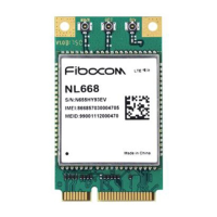
Presents visual representations of the NL668-LA series module's physical appearance.
Provides the precise mechanical dimensions of the module in millimeters.
Refers to external documentation for detailed PCB soldering and stencil design guidelines.
Points to external documentation for Surface Mount Technology (SMT) process parameters and requirements.
Directs users to external documentation for guidelines on carrier and storage procedures.
Details the CE conformance and compliance with EU directives for the device.
Lists supplementary documents and user guides relevant to the NL668-LA module.
Lists industry standards (e.g., 3GPP) that the product design adheres to.
| Brand | Fibocom |
|---|---|
| Model | NL668-LA Series |
| Category | Wireless modules |
| Language | English |