Appendix D How to Use PLC Function
VFD-E Series
Revision August 2006, 01EE, SW--PW V1.03/CTL V2.03 D-13
The figure above is common used oscillating circuit for indication light blinks or buzzer alarms. It
uses two timers to control On/OFF time of Y1 coil. If figure, n1 and n2 are timer setting of T1 and T2.
T is the base of timer (clock period)
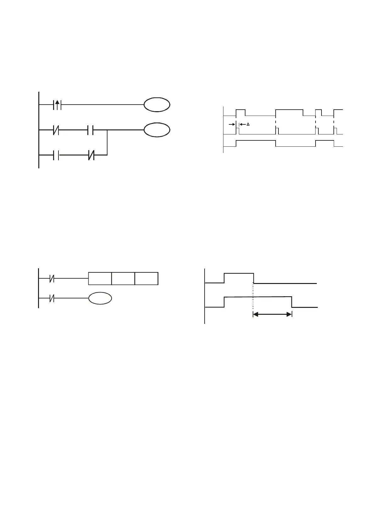
Example 9: Triggered Circuit
Y1
M0
X0
Y1
Y1
M0
M0
X0
M0
Y1
T
In figure above, the rising-edge differential command of X0 will make coil M0 to have a single pulse
of ӔT (a scan time). Y1 will be ON during this scan time. In the next scan time, coil M0 will be OFF,
normally close M0 and normally close Y1 are all closed. However, coil Y1 will keep on being ON and
it will make coil Y1 to be OFF once a rising-edge comes after input X0 and coil M0 is ON for a scan
time. The timing chart is as shown above. This circuit usually executes alternate two actions with an
input. From above timing: when input X0 is a square wave of a period T, output coil Y1 is square
wave of a period 2T.
Example 10: Delay Circuit
T10
X0
TMR
Y1
T10
K1000
TB = 0.1 sec
X0
Y1
100 seconds
When input X0 is ON, output coil Y1 will be ON at the same time due to the corresponding normally
close contact OFF makes timer T10 to be OFF. Output coil Y1 will be OFF after delaying 100
seconds (K1000*0.1 seconds =100 seconds) once input X0 is OFF and T10 is ON. Please refer to
timing chart above.
Example 11: Output delay circuit, in the following example, the circuit is made up of two timers. No
matter input X0 is ON or OFF, output Y4 will be delay.


 To Next Page
 Loading...
