© Gooligum Electronics 2015 www.gooligum.com.au
Baseline and mid-range PIC training and dev board operation guide Page 5
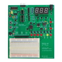
Plug your PICkit 2 or PICkit 3 programmer directly into the ICSP socket, with the arrow on the
programmer aligned with the arrow on the PCB (indicating pin 1).
You would normally use the PICkit 2 or PICkit 3 to power the training board. These programmers can
supply up to around 30 mA. If you need more current than this (up to 1 A), or if you wish to use the
training board without having a PICkit 2 or PICkit 3 attached, you can connect a regulated power supply
to the DC power socket.
This socket accepts a standard 5.5 mm barrel DC plug, with a 2.1 mm positive centre pin.
Note that there is no voltage regulator on the training board. A diode offers polarity protection, also
dropping the supply voltage by at least 0.6 V. Since most baseline and mid-range PICs (including those
used in the Gooligum tutorials) will work with a supply voltage of up to 5.5 V, you can safely use a power
supply of up to 6 V to power most
PICs with this training board – but it must be regulated!
A good choice for an external power supply is a 5 V regulated unit, which will supply around 4.3 V (after
the diode voltage drop) to the PIC.
The LEDs are connected, via jumpers and 330 Ω resistors, to PIC pins as marked on the circuit board.
Various PICs use different names for the same pin. For example, pin 2 of socket U2 is referred to as GP5
if you plug a 12F509 into that socket, RA5 if you plug in a 16F684, and RB5 if you use a 16F506. For
that reason, the LED connected to that pin is labelled ‘GP5 / RA5 / RB5’. On the other hand, pin 7 is
called RC3 on all 14-pin PICs, so the LED on that pin is labelled simply ‘RC3’.
LEDs are available on all output pins except RC4 and RC5.
To enable (connect) an LED, simply close its associated jumper.
Pushbutton switches are connected to GP/RA/RB2 and GP/RA/RB3/ MCLR via 1 kΩ isolation resistors.
They are active low: they will pull the input pin low when pressed (the isolation resistors ensure that the
PIC won’t be damaged if a button is pressed while the pin connected to it is configured as a high output).
The inputs are normally held high, while the switch is open, by either an external 10 kΩ pull-up resistor,
or an internal weak pull-up. Each external pull-up resistor is enabled by closing its associated jumper.
A 10 kΩ potentiometer and light-dependent resistor (LDR, or CDS photocell), forming one leg of a
potential divider, are available as analog voltage sources. Either can be connected, via jumper JP24, to pin
AN0 / CIN+ / C1IN+, to act as either an ADC or comparator input.
A second LDR can be connected, via jumper block JP25, to ADC input AN2 or comparator inputs C2IN+
or CIN- / C1IN-.
The board includes a 32.768 kHz oscillator, implemented with a watch crystal and CMOS inverter. Its
buffered output can be used to drive Timer0 (in counter mode), by using JP22 to connect it to the T0CKI
pin. It can also be used as an external signal to drive the processor clock, via jumper block JP20.
In a real PIC application, if you needed a 32.768 kHz clock, you’d be more likely to simply use a watch
crystal with the PIC’s internal oscillator. The training board includes a second 32.768 kHz crystal (with
load capacitors), which can be connected to OSC1 (on one side) via JP20 and to OSC2 (on the other
some PICs (mostly ‘LF’ variants) will only tolerate a supply of up to 3.6 V- you should limit your external power
supply to no more than 4 V if you are using one of these devices
 Loading...