positive variable supply will have an output of
about
-
0.2 Volts, and the negative supply an
output of about
+
0.2 Volts.
This can be useful in some test situations, where
it is is helpful if a voltage can be adjusted to zero
and a little beyond. If the utmost in stability is
required from the adjustable supplies, then the
diode pairs
D9-10
and
Dl
l-l 2 could be
jumpered. This would make the lowest voltage
setting obtainable 1.25 Volts, but the output
voltages would be more stable with changes in
power line voltage, load, and ambient
temperature.
6.
Turn OFF the 808 power switch, and remove its
power plug from the outlet. This completes the
ADJUSTMENT VOLTAGE EXPERIENCE. Have
you
r
instructor initial your Progress Guide.
PROTECTION CIRCUITRY
DISCUSSION
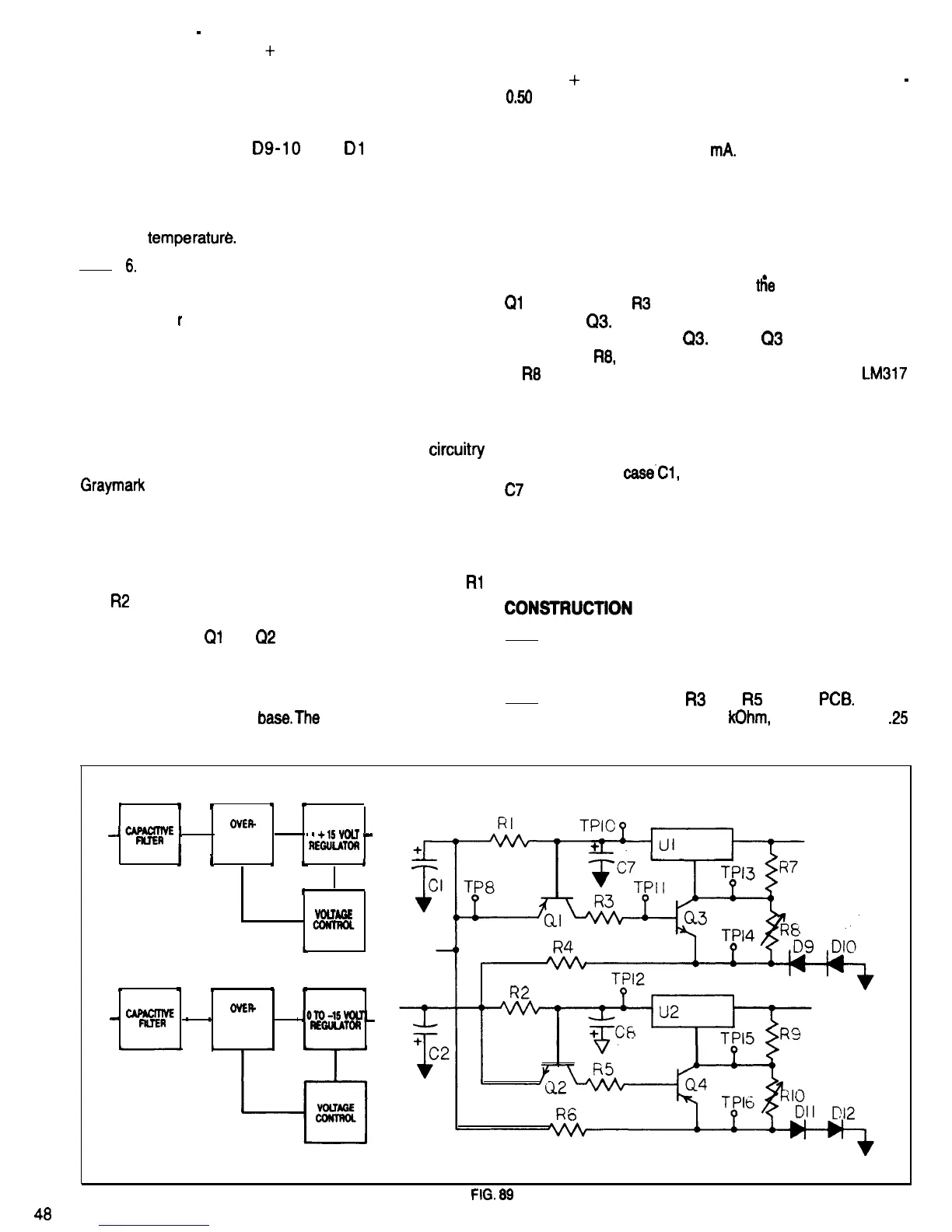
Figure 89 is a partial block diagram and schematic of the
808, with the external protection circuitry highlighted.
The overcurrent and over temperature protection
circuitty
built into the voltage regulators that are used in Your
Graymark
808 do a good job of protecting the regulators
themselves, but under some conditions over current
damage could occur to other power supply components.
With this in mind, circuitry has been designed into the 808
to give additional protection.
We have already talked about current sensing resistors
Rl
and
R2
and used them to determine the current flowing
through the voltage regulators in tests that were done
earlier. Transistors
Ql
and
Q2
monitor the voltage drop that
occurs across these resistors.
The collector current of a transistor depends on the voltage
applied from collector to emitter, and the current flowing
between the emitter and
base.The
emitter to base current
depends primarily on the voltage applied between the
transistors base and emitter, and secondarily on the
temperature of the transistor.
At normal operating temperatures, base current starts to
flow when the voltage of the base in respect to the emitter
is about
+
0.50 Volts for an NPN transistor, and about
-
050
Volts for a PNP transistor. With the transistor base and
emitter leads connected across a 1 Ohm resistors, base
current begins to flow when the current through the
resistors reaches about 500
mA.
As the base current of a transistor increases, the collector
current will increase as well. A given change in the base
current of a transistor results a larger change in the
collector current. We could say that as base current
increases in a transistor, resistance between the emitter
and collector of that transistor decreases. In the positive
adjustable power supply of the 808,
tl?e
collector current of
Ql
flows through
R3
and increases the base to emitter
voltage of
Q3.
This results in a drop in the emitter to
collector resistance of
Q3.
Since
Q3
is connected in
parallel with
R8,
the result is the same as if the resistance
of
R8
was reduced, and the output voltage of the
LM317
voltage regulator is reduced as well.
The voltage regulators can become unstable and cause
rapid changes or oscillations in the output voltage if there
is too much resistance or reactance between the filter
capacitor, in this
case’C1,
and the regulator input terminal.
C7
is provided to prevent this oscillation.
All the polarities are reversed in the over current protection
circuit for the negative adjustable power supply, but this
circuit operates in the same-manner as the one described
above.
1.
Be sure that the 808 power plug is not connected
to a power outlet. Refer to Fig. 90 for the following
steps.
2. Mount resistor
R3
and
R5
on the
PCB.
These
resistors are both 6.8
kQhm,
(blue-gray-red),
.25
Watt. Solder the resistor leads to the PCB and
cut off any excess length. Save one of these
.
t t
4
.
l
_-E,
,
OVER-
010
FIUER
CURRENT
I
3
+lS
VOU
-
DETECTOR
REGULAXM
1 1
\
&
4
B
l
VouhGE
.
*
4
\
,
.
,
OVER-
-
FILTER
’
’
CURRENT
1
~om-‘sw-
DETECTOR
REGUlAmR
48
FIG.
89

 Loading...