Section 4
4-27
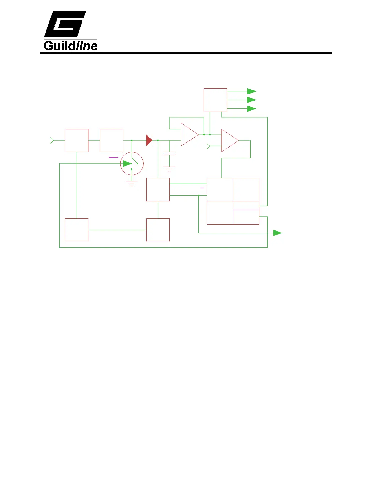
block of data comes from the digitized output of the integrator, after the integrator has been
halted at the end of the conversion cycle. The pause between conversions is 3.5 mS, which
allows ample time for the processor to compute the result before the next cycle begins.
CHARGE
BALANCE
SAMPLER
U4
MASTER
CLOCK
U7 & U1
CONVERSION
TIMER
U6 & U8
INTER-
PAUSE
1/2 U5 & U3
/D TRIGGER
1/2 U5
CONVERSION
Q
Q
CURRENT
MODE
SWITCH
U18,U19
PRECISION
CURRENT
SINK
U21,U20,R35
-7 VOLTS
-5.5 VOLTS
PRECISION
REFERENCES
U13,U12,
R18,R19,R20
V/I
CONVERTER
U11,
R10 to R13
R16,R17
HIGH SPEED
LOW NOISE
CURRENT
BUFFER
Q3,Q4
CR3
STOP
/
START
INTEGRATOR
U17
FAST
SWITCH
C18
TEFLON
INTEGRATOR
CAP
-
+
+
--
V
TRIP
U16
U15
FET BUFFER
AMP
LIMIT
DETECTOR
12-BIT
A/D
SERIAL CLOCK
SERIAL DATA
STATUS INT
IN
V
-1.5 VOLTS
CTR
(10mA)
TIMING UNIT
(OPTO-COUPLERS)
(OPTO-COUPLER)
Figure 4-10 : Charge Balance A/D Converter
The integrator in the converter is never reset (only halted), and the 22-bit conversion
consists of the 14-bit charge-balance counter, and the apparent 8-bit step the integrator has
taken between conversions.
In the approach taken, an input signal in the ±1 V range, always has two possible outputs,
that is:
1) (count) + (+step)
2) (count + 1) + (-step)
However, they both yield the same result because:
(+step) + (-step) = maximum possible swing of integrator (which is fixed)
= ADC Beta
It would be useful to refer to the schematic drawing 19502.01.04 and Figure 4-10 for the
following circuit descriptions.
 Loading...