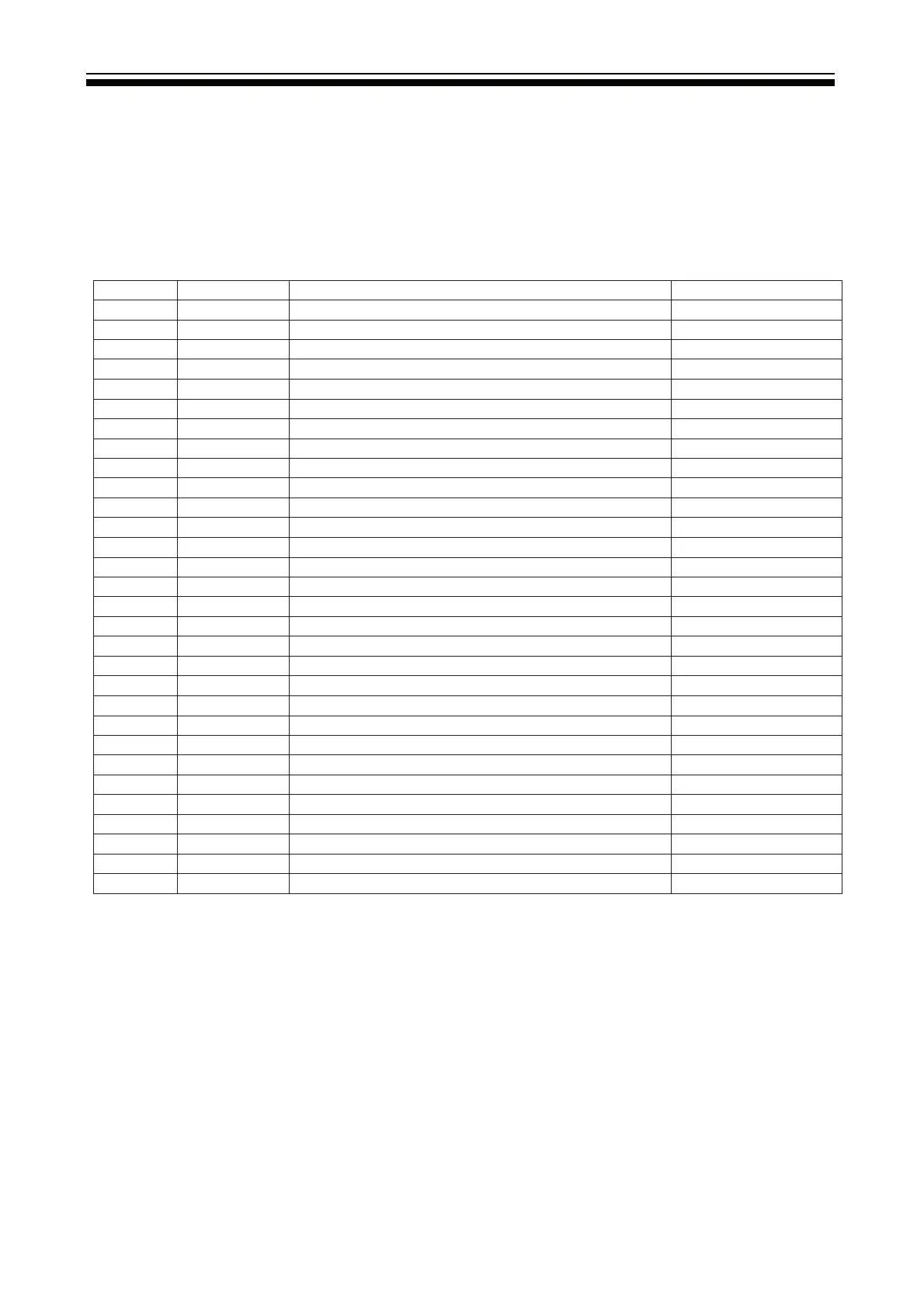
CN1
- 13 -
3-4-1 Function Description: Display the signal.
Pin No. Symbol Description Note
1 VCC Power supply: +12V
2 VCC Power supply: +12V
3 VCC Power supply: +12V
4 VCC Power supply: +12V
5 GND Ground
6 GND Ground
7 GND Ground
8 GND Ground
9 SELLVDS Select LVDS data format (2)
10 ODSEL Overdrive Lookup Table Selection (3)
11 GND Ground
12 RX0- Negative transmission data of pixel 0
13 RX0+ Positive transmission data of pixel 0
14 GND Ground
15 RX1- Negative transmission data of pixel 1
16 RX1+ Positive transmission data of pixel 1
17 GND Ground
18 RX2- Negative transmission data of pixel 2
19 RX2+ Positive transmission data of pixel 2
20 GND Ground
21 RXCLK- Negative of clock
22 RXCLK+ Positive of clock
23 GND Ground
24 RX3- Negative transmission data of pixel 3
25 RX3+ Positive transmission data of pixel 3
26 GND Ground
27 TST_AGE Aging Mode (4)
28 NC No connection (5)
29 GND Ground
30 GND Ground

 Loading...