74LCX32
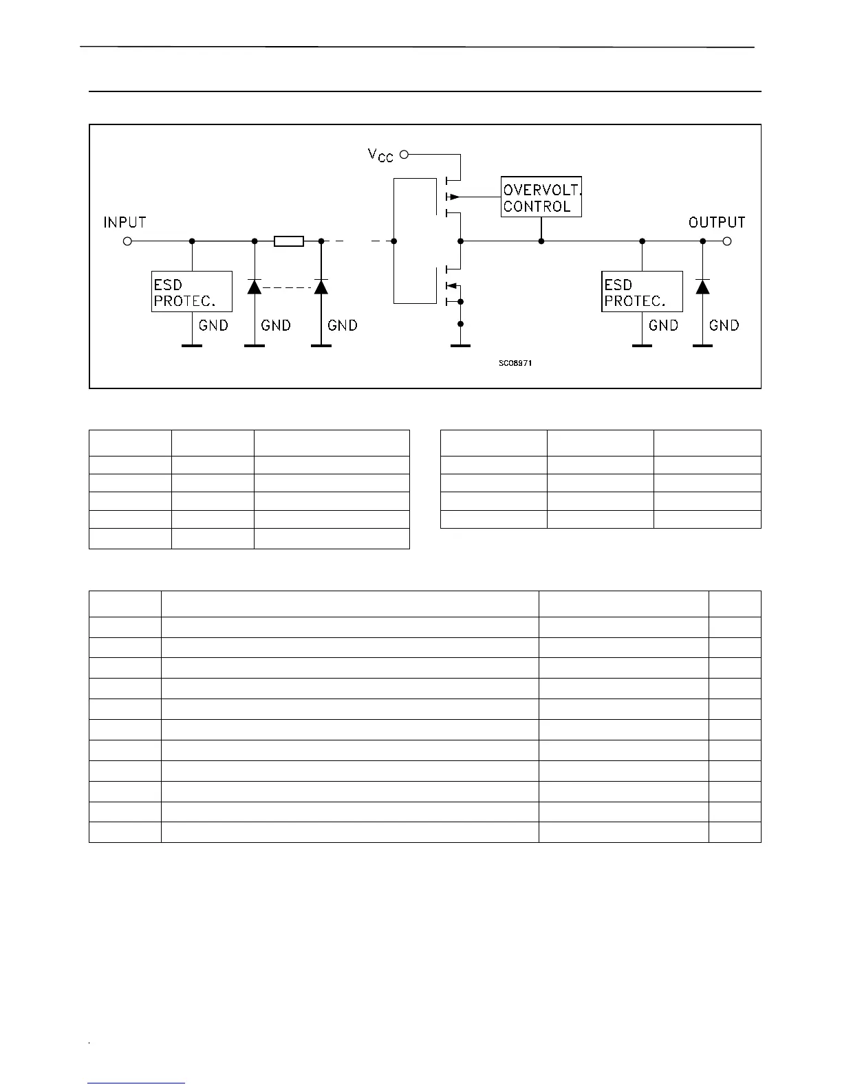
Figure 2: Input And Output Equivalent Circuit
Table 2: Pin Description Table 3: Truth Table
Table 4: Absolute Maximum Ratings
Absolute Maximum Ratings are those values beyond which damage to the device may occur. Functional operation under these conditions is
not implied
1) I
O
absolute maximum rating must be observed
2) V
O
< GND
PIN N° SYMBOL NAME AND FUNCTION
1, 4, 9, 12 1A to 4A Data Inputs
2, 5, 10, 13 1B to 4B Data Inputs
3, 6, 8, 11 1Y to 4Y Data Outputs
7 GND Ground (0V)
14
V
CC
Positive Supply Voltage
ABY
LLL
LHH
HLH
HHH
Symbol Parameter Value Unit
V
CC
Supply Voltage
-0.5 to +7.0 V
V
I
DC Input Voltage
-0.5 to +7.0 V
V
O
DC Output Voltage (V
CC
= 0V)
-0.5 to +7.0 V
V
O
DC Output Voltage (High or Low State) (note 1) -0.5 to V
CC
+ 0.5
V
I
IK
DC Input Diode Current
- 50 mA
I
OK
DC Output Diode Current (note 2)
- 50 mA
I
O
DC Output Current
± 50 mA
I
CC
DC Supply Current per Supply Pin
± 100 mA
I
GND
DC Ground Current per Supply Pin
± 100 mA
T
stg
Storage Temperature
-65 to +150 °C
T
L
Lead Temperature (10 sec)
300 °C
AVR3600 harman/kardon
 Loading...