Si4704/05
28 Preliminary Rev. 0.8
6. Pin Descriptions: Si4704/05-GM
Pin Number(s) Name Description
1, 20 NC No connect. Leave floating.
2 FMI FM RF input.
3 RFGND RF ground. Connect to ground plane on PCB.
4 LPI Loop antenna RF input.
5 RST Device reset (active low) input.
6 SEN Serial enable input (active low).
7 SCLK Serial clock input.
8 SDIO Serial data input/output.
9 RCLK External reference or crystal oscillator input.
10 VIO I/O supply voltage.
11 VDD Supply voltage. May be connected directly to battery.
13 ROUT Right audio analog line output.
14 LOUT Left audio analog line output.
15 DOUT Digital audio output data.
16 DFS Digital frame synchronization.
17 GPO3/DCLK General purpose output/digital bit synchronous clock or crystal oscillator
input.
18
GPO2/INT
General purpose output/interrupt.
19 GPO1 General purpose output.
12, GND PAD GND Ground. Connect to ground plane on PCB.
GND
PAD
1
2
3
17181920
11
12
13
14
6
7 8 9
4
5
16
10
15
GPO2/INT
VIO
DOUT
LOUT
ROUT
GNDRST
NC
LPI
RCLK
SDIO
VDD
FMI
RFGND
GPO3/DCLK
NC
GPO1
DFS
SCLK
SEN
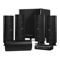
HS 2X0/230 Service Manual

 Loading...