39
DP65
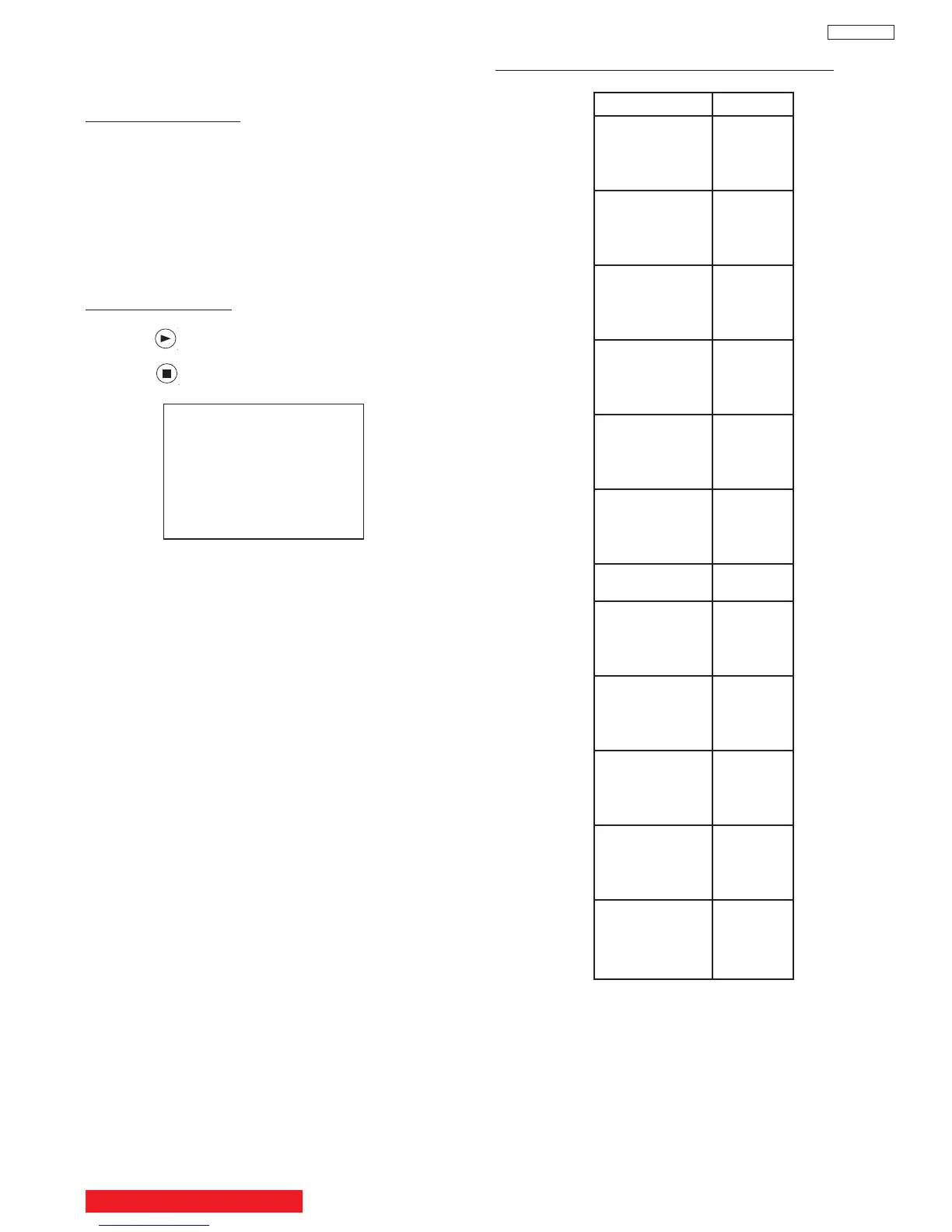
Parameter Normal
ADJ. DISP 0F
DEMO WAIT 00
INT. START 13
V. SQUEEZE 10
INT STEP 1 02
INT STEP 2 06
INT BAR 2D
INT DELAY 01
MGF STEP 1 50
MGF STEP 2 06
MGF BAR 1B
MGF DELAY 01
SEL. STAT. 00
LINE WID 7F
ADD LINE 09
SENSOR CK 00
PORT 0 07
PORT 1 06
PORT 2 05
PORT 3 04
PORT 4 03
PORT 5 02
PORT 6 01
PORT 7 00
AD LEVEL 03
CENT. BAL 01
E. DISPLAY 00
ADJ. TIMS 60
AD LEVEL 05
AD NOISE 0A
OVER. LF-H 01
OVER. LF-V 00
OVER. RI-H 00
OVER. RI-V 00
PHASE MOT 50
H. BLK-RV 0A
H. BLK-GV 03
H. BLK-BV 09
H. BLK-H 20
PON DELAY 0F
IR-CODE 00
INITIAL 50 9E
MGF 50 96
CENTER 50 FE
STAT 50 FE
DYNA 50 9F
2.12.1 MAGIC FOCUS Character Set-Up
This instruction should be applied when a new
Signal Block or complete chassis is being replaced.
Adjustment Preparation
(1) Receive NTSC RF or video signal.
(2) With Power off, PRESS and HOLD the SERVICE
ONLY button on SIGNAL PWB, then press the
Power On/Off, when picture appears release
SERVICE ONLY switch (Internal crosshatch is
displayed without conv. correction data).
(3) Set R/C to DCAM mode (refer to page 45).
(4) Press the DAY/NIGHT button 2 times for ROM READ
operation. Picture will appear with convergence
correction data.
Adjustment Procedure
(1) Press key on R/C. (One additional line appears
near the top and near the bottom.)
(2) Press key, then ADJ. PARAMETER mode is
displayed as following.
(3) Press CURSOR PAD
F or E to change the ADJ.
DISP. data.
(4) Press CURSOR PAD H to access DC parameter.
Change the data as shown on Table 1, DC
Parameter.
(5) Press Aspect key 2 times to write changed data into
EEPROM. (First press ADJ. PARAMETER/ROM
WRITE? is displayed for alarm. 2nd press, writes
data into EEPROM. Green dots appear after
completion of operation.)
(6) Press MUTE key 3 times to exit from ADJ.
PARAMETER mode.
ADJ. PARAMETER
ADJ. DISP.: 0F
DEMO WAIT: 1F
INT. START: 13
V. SQUEEZE: 10
TABLE 1. - Digital Convergence PARAMETER
BACK TO ADJUSTMENTS