HMCS47C,HMCS47CL---------------------------------------------------------
•
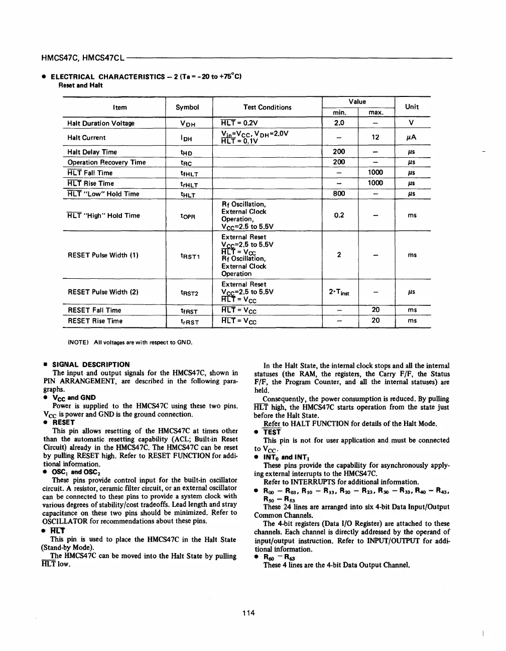
ELECTRICAL
CHARACTERISTICS - 2 (Ta =
-20
to
+75°C)
Reset
and
Halt
Value
Unit
Item
Symbol
Test Conditions
min.
max.
Halt
Duration Voltage
VOH
HLT
= 0.2V
2.0
-
V
Halt
Current
IOH
~Vee,
VOH=2.0V
-
12
#J,A
HLT=0.1V
Halt
Delay Time
tHO
200
-
#J,s
Operation Recovery Time
tRe
200
-
#J,s
HLT
Fall Time
tfHLT
-
1000
#J,s
HIT
Rise
Time
trHLT
-
1000
#J,s
HLT
"Low"
Hold
Time
tHLT
800
-
#J,s
Rf
Oscillation,
HLT
"High"
Hold
Time
tOPR
External Clock
0.2
ms
-
Operation,
Vee=2.5
to
5.5V
External
Reset
RESET
Pulse
Width (1)
tRST1
*tf=2.5
to
5.5V
L =
Voc
2
ms
Rf
Oscillation,
-
External Clock
Operation
External
Reset
RESET
Pulse
Width (2)
tRST2
~=2.5
to
5.5V
2'Tinst
-
#J,s
=
Vee
RESET Fall Time
tfRST
RIT =
Vee
-
20 ms
RESET
Rise
Time
trRST
ALi
=
Vee
-
20
ms
(NOTE) All voltages are with respect
to
GN
O.
•
SIGNAL
DESCRIPTION
The input and output signals for the
HMCS47C,
shown in
PIN ARRANGEMENT,
are
described in the following para-
graphs.
•
Vee
and GND
Power
is
supplied
to
the
HMCS4
7C
using these two pins.
Vee
is
power and GND
is
the ground connection.
• RESET
This pin allows resetting
of
the
HMCS47C
at times other
than the automatic resetting capability
(ACL; Built-in Reset
Circuit) already in the
HMCS47C.
The
HMCS47C
can be reset
by
pulling RESET high. Refer
to
RESET FUNCTION for addi-
tional information.
• OSC, and
OSC
2
These pins provide control input for the built-in oscillator
circuit. A resistor, ceramic filter circuit, or an external oscillator
can be connected
to
these pins
to
provide a system clock with
various degrees
of
stability/cost tradeoffs. Lead length and stray
capacitance on these two pins should be minimized. Refer
to
OSCILLATOR for recommendations about these pins.
•
R[T
This pin
is
used
to
place the
HMCS47C
in the Halt State
(Stand-by Mode).
The
HMCS47C
can be moved into the Halt State by pulling
HLTlow.
In the Halt State, the internal clock stops and
all
the internal
statuses (the
RAM,
the registers, the Carry F/F, the Status
F/F,
the Program Counter, and all the internal statuses) are
held.
Consequently, the power consumption
is
reduced.
By
pulling
HLT high, the
HMCS47C
starts operation from the state just
before the Halt State.
Refer to HALT
FUNCTION for details
of
the Halt Mode.
• TEST
This pin
is
not for user application and must be connected
to
Vee.
'
• INTo
and
INTI
These pins provide the capability for asynchronously apply-
ing external interrupts
to
the
HMCS47C.
Refer
to
INTERRUPTS for additional information.
•
Roo
- R
o3
,
RIO
- R
u
,
R20
- R
23
,
R30
- R
33
,
R40
- R
43
,
Rso
-
RS3
These 24 lines are arranged into six 4·bit Data Input/Output
Common Channels.
The 4-bit registers (Data I/O Register) are attached
to
these
channels. Each channel
is
directly addressed
by
the operand
of
input/output instruction. Refer
to
INPUT/OUTPUT for addi-
tional information.
•
R60
-
R63
These 4 lines are the 4-bit Data Output Channel.
114
 Loading...

