----------------------------~--------------------------HMCS47C,HMCS47CL
The 4·bit register (Data I/O Register)
is
attached to this
channel.
The channel
is
directly addressed by the operand
of
output
instruction.
Refer
to
INPUT/OUTPUT for additional infonnation.
•
Do
-
0
15
These lines are
16
l·bit
Discrete Input/Output Common
Tenninals.
The
l·bit
latches are attached
to
these tenninals. Each ter·
minal is addressed by the Y register. The
Do
to
D3
tenninals are
also addressed directly by the operand
of
input/output instruc·
tion. Refer to INPUT/OUTPUT for additional infonnation.
•
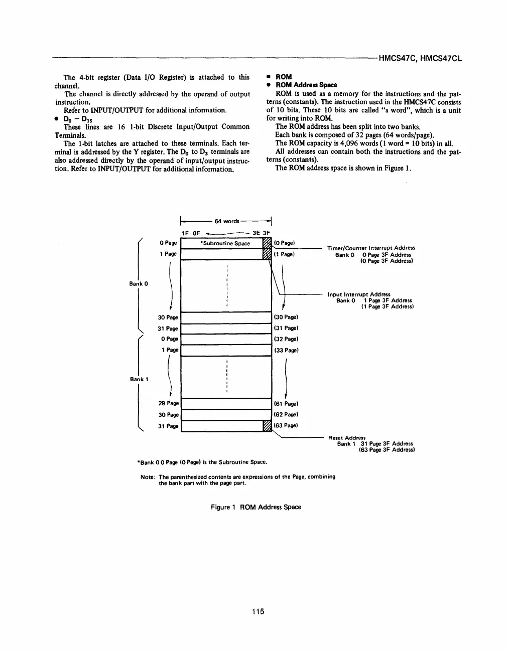
ROM
•
ROM
Address Space
ROM
is
used
as
a memory for the instructions and the pat·
terns (constants). The instruction used
in
the
HMCS47C
consists
of
10 bits. These 10 bits are called
"a
word". which
is
a unit
for writing into
ROM.
The
ROM
address has been split into two banks.
Each bank
is
composed
of
32 pages (64 words/page).
The
ROM
capacity
is
4,096 words
(1
word = 10 bits) in all.
All
addresses can contain
both
the instructions and the pat·
terns (constants).
The
ROM
address space
is
shown in Figure 1.
t-----
64
words----l
1F
OF
_3E3F
r
0 Page
1 Page
.'"'0 \
l
*Subroutine Space
1'°''''1
(1
Page)
1\1\
/
(30
Page)
(31
Pagel
30
Page
31
Page
r
0 Page
1 Page
_kI
~
l
(32
Page)
(33 Pagel
(61
Page)
(62
Page)
E (63
Page)
29 Page
30
Page
31
Page
*Bank 0 0 Page (0 Page)
is
the Subroutine Space.
Timer/Counter
I r.terrupt Address
Ban
k 0 0
Page
3F Address
(0 Page 3F Address)
Input Interrupt Address
Bank
0 1
Page
3F
Address
(1
Page
3F Address)
Reset Address
Bank 1 31 Page
3F Address
(63 Page 3F Address)
Note: The parenthesized contents are expressions of the Page. combining
the bank part with the page part.
Figure 1
ROM
Address Space
115
 Loading...

