LCO-III-------------------------------_
• REGISTERS
The LCD-UI has six 4-bit registers and two I-bit registers
available
to
the programmer. l-bit registers are Carry
F/F
and
Status
F/F.
They are explained in the following paragraphs.
•
Accumulator
(A; A Register)
and
Carry
F/F
(C)
The result
of
ALU operation (4 bits) and the overflow
of
the
ALU
are
put
into the accumulator and Carry F
/F.
Carry
F/F
can be set, reset
or
tested. Combination
of
the accumulator
and
Carry
F/F
can be right
or
left rotated. The accumulator is
the
main register for ALU operation and Carry
F/F
is used
to
store the overflow generated
by
ALU operation when the
calculation
of
two
or
more digits
(4
bits/digit) is perfonned.
• 8 Register
(8)
The result
of
ALU operation
(4
bits) is
put
into this register.
B register is used as a sub-accumulator
to
stack the data tempo-
rarily and also used as a counter.
• X Register (X)
The result
of
ALU operation
(4
bits) is
put
into this register.
X register
has
exchangeability for
SPX
register. X register
addresses the
RAM
me.
• SPX Register (SPX)
SPX
register has exchangeability for X register.
SPX
register is used
to
stack X register and expand the addres-
sing system
of
RAM
in combination with X register.
• Y Register (Y)
The result
of
ALU operation
(4
bits) is
put
into this register.
Y register has exchangeability for
Spy
register. Y register can
calculate itself simultaneously with transferring the data
by
bus
lines, which is usable for the calculation
of
two
or
more digits
(4 bits/digit).'
Y register addresses the
RAM
digit and I-bit
discrete input/output common terminals.
•
Spy
Register
(Spy)
Spy
register has exchangeability for Y register.
Spy
register
is
used
to
stack Y register and expand the
addreSSing
system
of
RAM
and I-bit discrete input/output common terminals in
combination with
Y register.
•
Stetul
F/F
(S)
Status F
/F
latches the result
of
logical
or
arithmetic opera-
tions (Not Zero, Overflow) and bit test operations. Status
F/F
affects conditional instructions (LPU, BR and CAL). These
instructions are executed only when Status F
/F
is
"I".
If
it
is
"0",
these instructions are skipped and Status F
/F
becomes
"I".
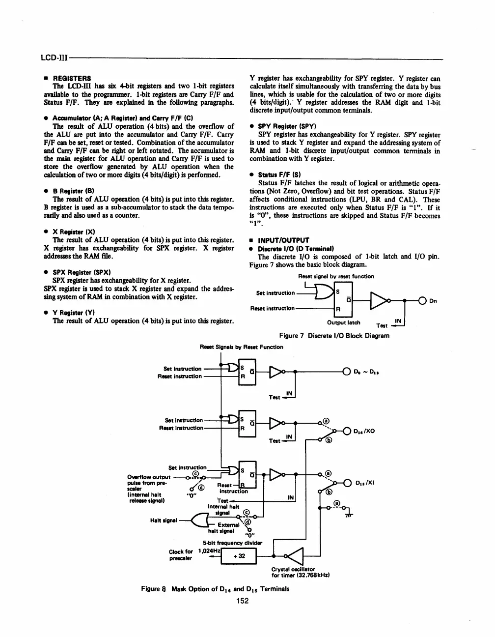
• INPUT/OUTPUT
•
Discrete
I/O
(0
Terminal)
The discrete I/O is composed
of
l-bit latch and I/O pin.
Figure 7 shows the basic block diagram.
Reset signal
bV
reset
function
Set
instruction
On
Reset
in.truction----~
Figure 7 Discrete
I/O
Block Diagram
Reset Signals
by
Reset
Function
Set
Instruction
Reset instruction
----i---1
Set
Instruction
---"'r-lI.-'
Reset Instruction
---If---I
Set
Instruction
Owrflow
outDUt
--6~
pulse
from
preo
-
j~
scaler
a
\!!I
(internal
halt
"0"
IN
rei
....
signal)
Test------!f---....:.:.,;.j
Internal
halt
~
ignal
@
Helt signal
~
External
.~
Clock
for
prescaler
halt
signal
"0"
Crystal oscilletor
for
timer
(32.768kHzl
Figure 8
Mask
Option
of
0
14
and
015
Terminals
152
Do
-On
DIS/XI
 Loading...

