----------------------------------
LCD-III
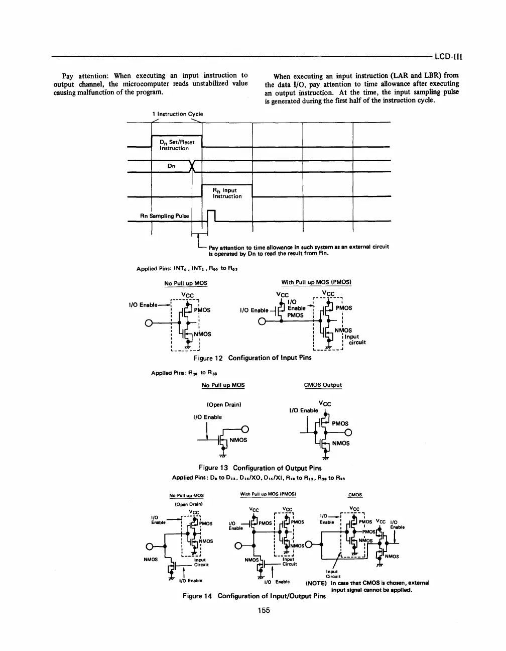
Pay attention:
When
executing an input instruction
to
output channel, the microcomputer reads unstabilized
value
causing malfunction
of
the program.
When
executing an input instruction (LAR and LBR) from
the data
I/O, pay attention to time allowance after executing
an output instruction. At the time, the input sampling pulse
is
generated during the first half
of
the instruction cycle.
1 Instruction Cycle
/'
-..
on
Set/Reset
-
Instruction
On
J
Rn Input
Instruction
Rn Sampling Pulse
I
T.
m
Pay
attention
to
time allowance
In
such syste as
is
operated
by
On
to
read
the
result from Rn.
an extarna circuit
Applied Pins: INTo.
INT,.
Roo
to
Rn
No
Pull
up
MOS
VCC
I/O
E~'
[--tf,---tos
I
NMOS
I I
: :
'"----
--~
With Pull
up
MOS
(PMOS)
Figure 12 Configuration
of
Input
Pins
Applied Pins:
R30
to
Rn
No Pull
up
MOS
(Open Drain)
I/O Enable
CMOS
Output
VCC
~r-
IroEi~b
4~NMO;
Figure 13 Configuration
of
Output
Pins
Applied Pins: 0
0
to
0
13
• O'4/XO.
D,s/XI.
R,o
to
Ru.
R20
to
Rn
No Pull
upMOS
(Open Drain)
I/O
---:--~~!:~~
Enable I
PMOS
I •
I I
:
~MOS
I I
: :
f..
____
..1
Input
h-eirCUit
t
With
Pull
up
MOS
(PMOS)
Vee Vee
r--i---
1
PMOS:
PMOS
I I
I
I I
I J
I . I
: NMOS
I I
""----.1
NMOS
~
g:~~it
1
Input
Circuit
I/O
Enable
~
I/O Enable
I/O
Enable
(NOTE)
In
case
that
CMOS
is
chosen. external
input
signal cennot
be
applied.
Figure 14 Configuration
of
Input/Output
Pins
155
 Loading...

