LCO-IV--------------------------------
14. Current
that
flows in
the
input/output
circuit and.
in
the
power supply circuit for
LCD
is
excluded. The standby supply
current
111
il
the
supply
at
Vee
= 2.5
to
3.3V
in
"Halt"
state
in
the
case
that
the crystal oscillation for timer
is
not
selected.
The
lupply
current
when supply voltage fails
to
the
Halt Duration Voltage
is
calledUHalt
Current"
(I
DH
I.
(shown
in
ELECTRICAL CHARACTERISTICS
-21.
15. The voltage
that
drops between
the
power supply terminals
(Vee,
V.,
V
2
,
Vsl
and
each common
or
segment
output
terminal.
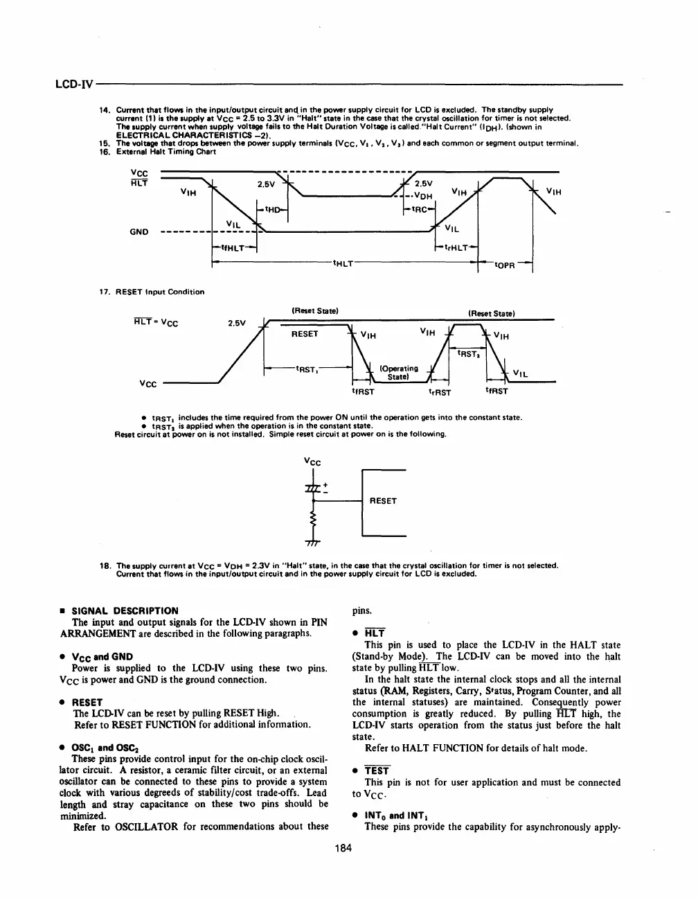
16. External Halt Timing Chart
VCC
HLT
2.5V:t"-
-----
-----------~---2.5V
.--------------~.-
--VDH
tH
tRC
GND
~--------------------tHLT----------------------+--
17. RESET
Input
Condition
(Reset Statel
H"Cf=
VCC
VCC
tfRST
tfRST
trRST
• tRST.
includes
the
time required from
the
power ON until
the
operation gets into
the
constant
state
.
• tRST2
is
applied when
the
operation
is
in
the
constant
state.
Reset circuit
at
power on
is
not
installed. Simple reset circuit
at
power
on
is
the
following.
Vee
+
RESET
18.
The supply
current
at
Vee
= VOH = 2.3V
in
"Halt"
state,
in
the
case
that
the
crystal oscillation for timer
is
not
selected.
Current
that
flows in
the
input/output
circuit
and
in
the
power supply circuit for
LCD
is
excluded.
• SIGNAL DESCRIPTION
The input and
output
signals for the LCD-IV shown in PIN
ARRANGEMENT are described
in
the following paragraphs.
•
VccandGND
Power
is
supplied to the
LCD-IV
using these two pins.
Vee
is
power and GND
is
the ground connection.
•
RESET
The
LCD-IV
can
be
reset by pulling RESET High.
Refer
to
RESET FUNCTION for additional information.
•
OSC
1
and
OS~
These pins provide control input for the on-chip clock oscil·
lator circuit. A resistor, a ceramic filter circuit, or an external
oscillator can be connected to these pins
to
provide a system
clock with various degreeds
of
stability/cost trade-offs. Lead
length and stray capacitance on these two pins should be
minimized.
Refer to
OSCILLATOR for recommendations about these
184
pins.
•
HLT
This pin
is
used to place the LCD-IV
in
the HALT state
(Stand·by Mode). The
LCD-IV
can be moved into the halt
state by pulling HLT low.
In the halt state the internal clock stops and all the internal
status
(RAM,
Registers, Carry, Status, Program Counter, and all
the internal statuses) are maintained.
Consequently power
consumption
is
greatly reduced.
By
pulling
HIT
high, the
LCD·IV starts operation from the status just before the halt
state.
Refer to HALT
FUNCTION for details
of
halt mode.
• TEST
This pin
is
not for user application and must
be
connected
to
Vee.
• INTo
and
INTI
These pins provide the capability for asynchronously apply-


 To Next Page
 Loading...