---------------------------------
LCD-IV
Reset Signals by Reset Function
Set instruction
~-.-CL...""
Reset instruction
--+---f
Set
instruction
--..-
.............
Reset
instruction--t---t
Set
instruction
Overflow
output
---<>ill
pulse from pre-
Do
....
D.
s
DIS/XI
scaler
(internal
halt
release signal! Test
____
-t-
___
IN..J
Internal halt
~.@
Halt signal
~
External'-@
halt
~:;~~~I
'''0
"0"
Clock for
pre-scaler
Crystal
oscillator
for timer (32.768kHz)
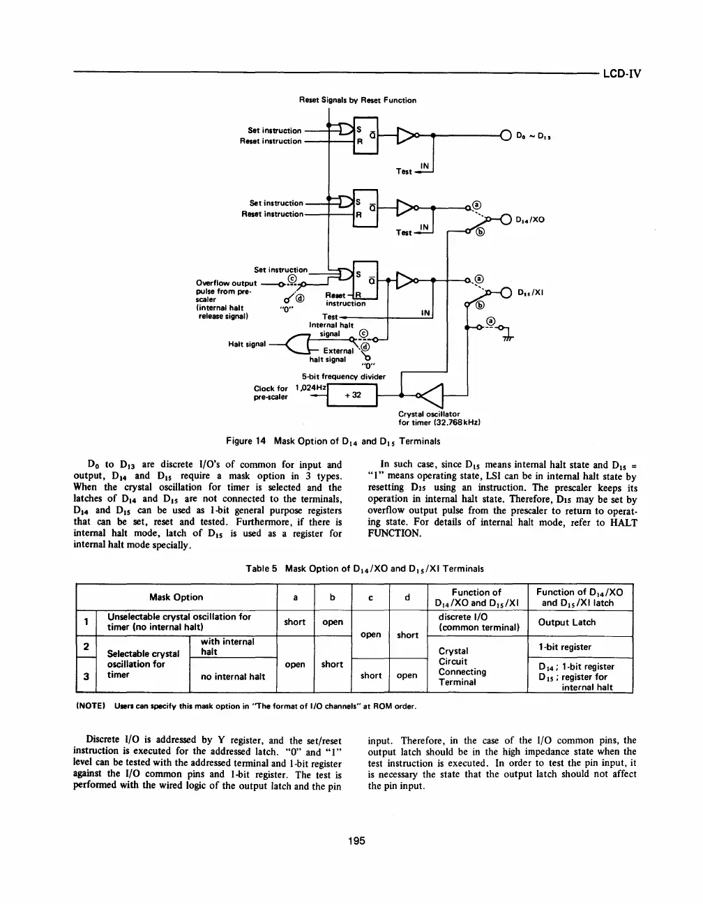
Figure 14
Mask
Option of
DI4
and
DIS
Terminals
Do
to
D13
are discrete I/O's
of
common for input and
output,
DI4
and
DIS
require a mask option
in
3 types.
When the crystal oscillation for timer
is
selected and the
latches
of
DI4
and
DIS
are
not
connected
to
the terminals,
DI4
and D
I5
can be used
as
l-bit general purpose registers
that can
be
set, reset and tested_ Furthermore,
if
there is
internal halt mode, latch
of
DIS
is
used
as
a register for
internal halt mode specially.
In such case, since
DIS
means internal halt state and
DIS
=
"I"
means operating state, LSI can be
in
internal halt state by
resetting
DIS
using an instruction. The pre scaler keeps its
operation in internal halt state. Therefore,
DIS
may be set
by
overflow
output
pulse from the prescaler
to
return
to
operat-
ing state.
For
details
of
internal halt mode, refer
to
HALT
FUNCTION.
Table 5
Mask
Option of D
I4
/XO and Dis/XI Terminals
Mask
Option
a
b
d
Function of
Function of D
I4
/XO
c
D
I4
/XO and Dis/XI
and Dis/XI latch
1
Unselectable crystal oscillation for
short
open
discrete I/O
Output
Latch
timer (no internal halt)
(common terminal)
open
short
2
with internal
1-bit register
Selectable crystal
halt
Crystal
I--
Circuit
oscillation for open short
D
14;
1-bit register
3
timer
no internal halt
short
open
Connecting
DIs;
register for
Terminal
internal
halt
(NOTE) Users can specify this mask
option
in
"The
format
of
I/O channels"
at
ROM
order.
Discrete I/O
is
addressed by Y register, and the set/reset
instruction
is
executed for the addressed latch.
"0"
and
"I"
level can be tested with the addressed terminal and I-bit register
against the
I/O common pins and I-bit register. The test
is
performed with the wired logic
of
the output latch and the pin
195
input. Therefore, in the
case
of
the I/O common pins, the
output latch should be
in
the high impedance state when the
test instruction
is
executed. In order to test the pin input, it
is
necessary the state that the output latch should
not
affect
the pin input.


 To Next Page
 Loading...