LCO-IV----------------------------------------------------------------
In
case
of
the instructions which consists
of
a simultaneous
Read/Write
opera~ions
of
RAM
(exchange
of
RAM
and a
regis-
ter), the writing data doesn't affect the reading data because the
read operation
is
followed by the write operation.
RAM
bit manipulation
is
usable, which performs any bit set
(SEM), reset (REM)
or
test (TM)
of
the addressed
RAM.
Bit
assignment
is
made by the program
as
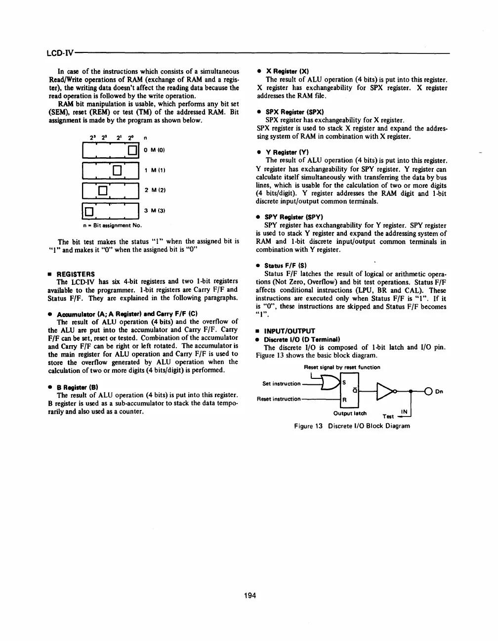
shown below.
2
3
22
21
20
n
I
: :
:01
OM
(0)
I :
:0:
I
1
M(1)
I
:0:
: I
2 M (2)
10:
:-
:
I
3
M(3)
n - Bit assignment
No.
The bit test makes the status
"I"
when the assigned bit
is
"I"
and makes it
"0"
when the assigned bit
is
"0"
• REGISTERS
The
LCD-IV
has
six
4-bit registers and two I-bit registers
available
to
the programmer. I-bit registers are Carry
F/F
and
Status F/F_ They are explained in the following paragraphs.
• Accumulator (A; A Register)
and
Carry
F/F
(C)
The
result
of
ALU
operation (4 bits) and the overflow
of
the
ALU
are
put into the accumulator and Carry F/F. Carry
F/F
can be set, reset
or
tested. Combination
of
the accumulator
and Carry F/F can be right
or
left rotated. The accumulator
is
the
main
register for
ALU
operation and Carry F
/F
is
used
to
store the overflow generated by
ALU
operation when the
calculation
of
two
or
more digits (4 bits/digit)
is
performed.
• 8 Register (8)
The
result
of
ALU
operation (4 bits)
is
put into this register.
B register
is
used
as
a sub-accumulator to stack the data tempo-
rarily and also used as a counter.
• X Regilter (X)
The result
of
ALU
operation (4 bits)
is
put into this register.
X register has exchangeability for
SPX
register. X register
addresses the
RAM
file.
• SPX Register (SPX)
SPX
register has exchangeability for X register.
SPX
register
is
used
to
stack X register and expand the addres-
sing system
of
RAM
in combination with X register.
• V Register (V)
The result
of
ALU
operation (4 bits)
is
put into this register.
Y register has exchangeability for
Spy
register. Y register can
calculate itself simultaneously with transferring the data by bus
lines, which
is
usable for the calculation
of
two
or
more digits
(4 bits/digit).
Y register addresses the
RAM
digit and I-bit
discrete input/output common terminals.
• SPY Register (SPV)
Spy
register has exchangeability for Y register.
Spy
register
is
used
to
stack Y register and expand the addressing system
of
RAM
and I-bit discrete input/output common terminals in
combination with
Y register.
•
Status
F/F
(S)
Status F/F latches the result
of
logical
or
arithmetic opera-
tions (Not Zero, Overflow) and bit test operations. Status
F/F
affects conditional instructions (LPU,
BR
and CAL). These
instructions are executed only when
Status F
/F
is
"I".
If
it
is
"0",
these instructions are skipped and Status F
/F
becomes
"I".
• INPUT/OUTPUT
•
Discrete I/O
(0
Terminal)
The discrete I/O
is
composed
of
l-bit latch and I/O pin.
194
Figure
13
shows the
basic
block diagram.
Reset signal
by
reset function
Set instruction
Reset
instruction-----t
Output latch
Test
Figure 13 Discrete I/O Block Diagram
On


 To Next Page
 Loading...