------------------------------------------------------------------LCO-IV
Subroutine
Jump
to
Bank 0
•
RAM
•
LAI
15
..
--LA A 7
~~PU
5)
CAL
3F;
•
LAI
15
LBA
'-LAA
: COMB
'.LPU
31
1
CAL
3F
J
A,o =
"1"
(A,o =
"0")
CALL
5-3F
(Subroutine
Jump
to
Bank 0 5-3F (5-3F))
A,o =
"1"
(A,o =
"0")
CALL
31-3F
(Subroutine
Jump
to
Bank 0 31-3F (31-3F))
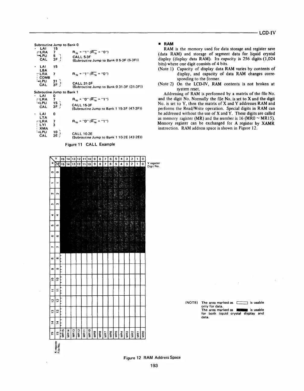
RAM
is
the memory used for data storage and register save
(data RAM) and storage
of
segment data for liquid crystal
display (display data RAM). Its capacity
is
256 digits (1,024
bits) where one digit consists
of
4 bits.
(Note
I)
Capacity
of
display data
RAM
varies
by
contents
of
display, and capacity
of
data
RAM
changes corre-
sponding
to
the former.
Subroutine
Jump
to
Bank 1
(Note 2) On the LCD-IV,
RAM
contents
is
not
broken
at
system reset.
Addressing
of
RAM
is
performed by a matrix
of
the file No.
and the digit No. Normally
the
file No.
is
set
to
X and
the
digit
No.
is
set
to
Y, then the matrix
of
X and Y addresses RAM and
performs the Read/Write operation. Special digits in RAM can
be addressed without the use
of
X and
Y.
These digits are calJed
as
memory ragister (MR) and the number
is
16
(MRO
- MR 15).
Memory register can be exchanged for A register by XAMR
instruction.
RAM
address space
is
shown in Figure 12.
•
LAI
0
'-LAA
7
~.LPU
15)
CAL
3F
J
LAI
0
LTA
-LAA
7
LVI
3
XMA
·LPU
10
)
CAL
2E J
A,o =
"0"
(R,;;
=
"1")
CALL
15-3F
(Subroutine
Jump
to
Bank 1 15-3F (47-3F))
A,o =
"0"
(A,o =
"1")
CALL
10-2E
(Subroutine
Jump
to
Bank 1 10-2E (42-2E))
Figure
11
CALL Example
Y register
Digit
No.
Figure
12
RAM
Address Space
193
(NOTE) The area marked
as
c=:=:J
is
usable
only
for
data.
The area marked
as
_
is
usable
for
both
liquid
crystal display and
data.



 To Next Page