----------------------------------------------------------------HMCS404C
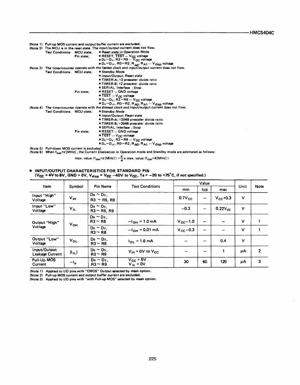
(Note
1)
Pull-up MOS
current
and
output
buffer
current
are excluded.
(Note 2)
The
MCU
is
in
the
reset state. The
input/output
current
does
not
flow.
Test Conditions:
MCU
state;
• Reset state in Operation Mode
Pin state; • RESET. TEST ...
VfX
voltage
.0.-0
3
•
R3-R9
...
VfX
voltage
.0.-0
...
RO-R2.
R
AO
•
RA1
... Vdisp voltage
(Note 3)
The
timer/counter
operate
with
the
fastest clock and
input/output
current
does
not
flow.
Test
Conditions:
MCU
state;
• Standby Mode
•
Input/Output;
Reset
state
• TIMER-A; +2 prescaler divide ratio
• TIMER-8; +2 prescaler divide ratio
• SERIAL Interface ;
Stop
Pin
state;
• RESET ... GND voltage
• TEST ... V fX voltage
•
0.-0
3
•
R3-R9
...
VfX
voltage
•
0.-0
...
RO-R2.
RAO.
RA1
... Vdisp voltage
(Note 4)
The
timer/counter
operate
with
the
slowest clock
and
input/output
current
does
not
flow.
Test
Conditions:
MCU
state;
•
Standby
Mode
•
Input/Output;
Reset
state
• TIMER-A;
+2048
prescaler divide ratio
• TIMER-8;
+2048
prescaler divide ratio
• SERIAL
Interface;
Stop
Pin
state;
• RESET.··· GND voltage
.TEST
... VfX voltage
• D.
-0
3
•
R3-
R9 ...
VfX
voltage
•
0.-0
...
RO-R2.
AAO.
AA1
... Vdisp voltage
(Note 5) Pull-down
MOS
current
is
excluded.
(Note 6) When·fosc=x[MHzl.
the
Current Dissipation
in
Operation
mode
and Standby mode are estimated as follows:
max. value (fos
c
=x[MHz])
=~x
max. value (fos
c
=4[MHz])
• INPUT/OUTPUT CHARACTERISTICS FOR STANDARD PIN
(Vee =
4Vto
6V.
GND =
OV,
VdilP = Vee
-40V
to
Vee,
Ta
=
-20
to
+75°C,
if
not
specified.)
Item Symbol
Pin
Name
Test Conditions
Input
"High"
V
1H
Do
-
03,
Voltage
R3
-
R5,
R9
Input
"low"
V
1L
Do
-
03,
Voltage
R3-
R5,
R9
Do
-
03,
Output
"High"
V
OH
R3-
R8
-IOH
=
1.0mA
Voltage
Do
-
03,
-IOH
= 0.01
mA
R3-
R8
Output
"low"
VOL
Do
-
03,
IOL = 1.6
mA
Voltage
R3-
R8
Input/Output
\lILI
DO
-
03,
Yin =
OV
to
VCC
leakage Current
R3-
R9
Pull-Up
MOS
-Ip
Do
-
03,
Vee - 5V
Current
R3-
R9
Yin =
OV
(Note
1)
Applied
to
I/O pins with "CMOS"
Output
selected
by
mask
option.
(Note 2) Pull-up
MOS
current
and
output
buffer
current
are excluded.
(Note 3) Applied
to
I/O pins with
"with
Pull-up MOS" selected
by
mask
option.
225
Value
min
typ
0.
7V
ee
-
-0.3
-
Vee-
1
.
O
-
Vee-
0
.
3 -
-
-
-
-
30
60
Unit
Note
max
Vee+
0
.
3
V
0.
22V
cc
V
-
V 1
-
V 1
0.4
V
1
p.A
2
120
p.A
3


 To Next Page
 Loading...