stances such as temperature, humidity and dust,
and
the
control of submaterials,like gas, and pure
water used
in
a manufacturing process, are inten-
sively executed.
Dust control is essential to realize higher integra-
tion and higher reliability of devices.
At
Hitachi,
maintenance and improvement of cleanliness at
manufacturing sites is accomplished through
QUALITY ASSURANCE
attention to buildings, facilities, air conditioning
systems, delivered materials,
clothes,
work
envir-
onment, and periodic inspection of floating dust
concentration.
3.3.3
Final
Product
Inspection and Reliability
Assurance
(1) Final Product Inspection
Lot inspection is done by the quality assurance
Process
Control
Point
Purpose
of
Control
Purchase
of
Material
Wafer,
I--
Surface
Oxidation
Frame
Package
Inspection
on
Surface
Oxidation
Photo
Resist
Inspection
on
Photo
Resist
<>
Pac
Level Check
Diffusion
Inspection
on
Diffusion
<>
pac
Level Check
Evaporation
Inspection
on
Evaporation
<>
Pac
Level Check
Wafer
Inspection
Inspection
on
Chip
Electrical Characteristics
Chip
Scribe
Inspection
on
Chip
Appearance
<>
Pac
Lot
Judgement
Assembling
<>
Pac
Level Check
Inspection
after
Assembling
<>
Pac
Lot
Judgement
Sealing
<>
pac
Level Check
Final Electrical Inspection
<>
Failure Analysis
Appearance Inspection
Sampling Inspection on
Products
Receiving
Shipment
Wafer
Oxidation
Photo
Resist
Diffusion
Evapora·
tion
Wafer
Chip
Characteristics, Appearance
Appearance, Thickness
of
Oxide
Film
Dimension, Appearance
Diffusion
Depth, Sheet
Resistance
Gate
Width
Characteristics
of
Oxide
Film
Breakt.:own Voltage
Thickness
of
Vapor
Film,
Scratch,
Contamination
Thickness,
VTH
Characteris·
tics
Electrical Characteristics
Appearance
of
Chip
Assembling Appearance
after
Chip
Bonding
Sealing
Marking
Appearance
after
Wire
Bonding
Pull Strength, Compression
Width,
Shear Strength
Appearance
after
Assembling
Appearance
after
Sealing
Outline,
Dimension
Marking
Strength
Analysis
of
Failures, Failure
Mode, Mechanism
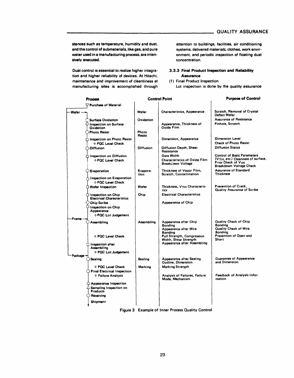
Figure 3 Example
of
Inner
Process
Quality Control
23
Scratch, Removal
of
Crystal
Defect Wafer
Assurance
of
Resistance
Pinhole, Scratch
Dimension Level
Check
of
Photo
Resist
Diffusion
Status
Control
of
Basic Parameters
(VTH,
etc.) Cleanness
of
surface,
Prior
Check
of
VIH
Breakdown Voltage Check
Assurance
of
Standard
Thickness
Prevention
of
Crack,
Quality Assurance
of
Scribe
Quality Check
of
Chip
Bonding
Quality
Check
of
Wire
Bonding
Prevention
of
Open and
Short
Guarantee
of
Appearance
and Dimension
Feedback
of
Analysis
Infor·
mation
 Loading...

