HD614POSOS--------------------------------------------------------------
~
.5
c:
'e
:r
0
l'
6
T.!...:zJ
-
~75°C
5
vcJ-5.~V-
~
4
..,'"
./
---
~
3
/
./
~C
C-
4
.
5V
Ih
/'
2
~
V
,I. V
~~
",
1/
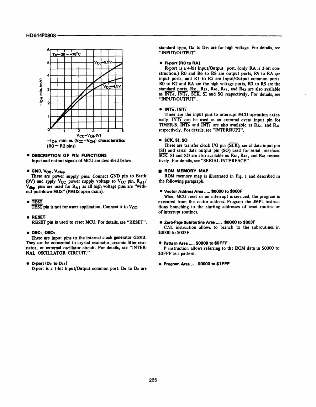
o 2 3 4 5
VCC-VOH(V)
-IOH
min.
\II. (Vcx:-VOH) characteristics
(RO
-
R2
pins)
• DESCRIPTION
OF
PIN FUNCTIONS
Input
and
output signals
of
MCU
are described below.
• GND,
Vee,
Vdl.,
These are power supply pins. Connect
GND
pin
to
Earth
(OV)
and apply
Vee
power supply voltage to
Vee
pin. RAI/
V diIp
pins
are used for RAI
as
all
high voltage pins are "with-
out pull-down MOS" (pMOS open drain).
•
TEST
TEST
pin is
not
for users application. Connect
it
to
Vee.
•
RESET
RESET pin
is
used
to
reset
MCU.
For details,
see
"RESET".
•
OSCI,
OSC2
These are input pins
to
the internal clock generator circuit.
They can be connected
to
crystal resonator, ceramic filter
reso-
nator,
or
external oscillator circuit. For details,
see
"INTER-
NAL OSCILLATOR CIRCUIT."
• D-port
(Do
to
015)
D-port
is
a I-bit Input/Output common port.
Do
to
Ih
are
266
standard type,
D4
to DIs are for high voltage. For details,
see
"INPUT/OUTPUT".
•
R-port
eRO
to
RA)
R-port
is
a 4-bit Input/Output port. (only
RA
is
2-bit con-
struction.)
RO
and
R6
to R8 are output ports, R9
to
RA
are
input ports, and RI
to
RS
are Input/Output common ports.
RO
to R2 and
RA
are the high voltage ports,
R3
to R9 are the
standard ports.
iU2,
R33,
R40, R41,
and
R42
are also available
as
INTo, INTI,
SCK.,
SI and
SO
respectively. For details, see
"INPUT/OUTPUT".
• INTo. INTI
These are the input pins to interrupt
MCU
operation exter-
nally. INTI can be used
as
an external event input pin for
TIMER-B.
INTo
and INTI are also available
as
R32,
and
R33
respectively. For details,
see
"INTERRUPT".
•
SCK,SI,SO
These are transfer clock I/O pin
(SCK),
serial data input pin
(SI) and serial data output pin (SO) used for serial interface.
SCI{,
SI
and SO
are
also available
as
R40,
R41,
and
R42
respec-
tively. For details,
see
"SERIAL INTERFACE".
• ROM MEMORY MAP
ROM
memory map
is
illustrated in
Fig.
I and described in
the following paragraph.
•
Vector
Address Area .....
$0000
to
$OOOF
When
MCU
reset or an interrupt is serviced, the program
is
executed from the vector address. Program the JMPL instruc-
tions branching to the starting addresses
of
reset routine or
of
interrupt routines.
• Zero-Page
Subroutine
Area .....
$0000
to
$OO3F
CAL instruction allows
to
branch to the subroutines in
$0000 to $003F.
•
Pattern
Area
.....
$0000
to
$OFFF
P instruction allows referring to the
ROM
data in $0000 to
$OFFF
as
a pattern.
• Program Area .....
$0000
to
$1FFF


 To Next Page
 Loading...