HD44857E---------------
The
HD448S7E
is
an
evaluation
chip
for
4-bit
sinaJe-chip
microcomputer,
HMCS40
series.
Its
·function
is
equivalent
to
HMCS47C
except
that
it
doesn't
contain
ROM
and
RAM.
In-
stead,
it
has
the
function
to
address
external
memory,
program
memory
(ROM
or
RAM)
and
data
memory
(RAM).
User
can
handle
this
evaluation
chip
by
writing
program
into
external
program
memory
as
well
as
the
HMCS40
series
chip
in
which
program
has
been
written.
The
HD448S7E
provides
addresslinstruction
pins
(Ao/O
I
to
At/O
lo
, Alol
All
terminals)
for
the
external
program
memory,
and
addresslbus
pins
(YI/S
..
to
Y./S
w
X/Sal
to
X./S
u
),
timing
signal
"'1'
"'a
pins
for
accessing
data
RAM.
",
and
TSTP
pins
are
required
for
debugging
programs,
and
CMOS
and
DIE
pins
for
selecting
applicable
chips.
• APPLICABLE CHIPS
HMCS42C,43C.44C,45C,46C,47C
• FUNCTION
•
Instruction Characteristics etc.; Same
as
the HMCS47C
•
Address Extemal
ROM
(max;
4k
words)
• Access External Data RAM (max;
256
digits)
• CMOS/PMOS Selecting Input Pin
for
evaluating PMOS
•
Timer Stop Input
• 1/0 EnablelDisable Selecting Input Pin at Halt
•
External ROMIRAM Access Pin; CMOS Pin
All Output Pins except these
are
Open Drain Output.
• Input Pin; Input
with
no Pull up MOS
• PIN
NAME
(1)
AoIOl
to
A,IO,o
: Access pins
for
user program external
memory. Divide 1 instruction
cycle by
two. The
first
half is the address from
Ao
to
At
and the latter half
is
instruction
(2)
A,oIA"
inputs
from
0,
to
0,
o'
: Access pins
for
external user program
memory. Divide
1 instruction cycle by
two. The
first
half is
Al
0 and the latter
half
Is
A'I'
(3) A
'I'
: Unusable.
Be
"open"
always.
(4) X
1
/S
2
,
to
X./S
u
:
Access pins
for
data RAM. Divide 1 in-
struction cycle by two. The
first
half
(X
1
to
X.)
Is
for
selecting RAM file and the
latter half
(S
21
to
S 24)
Is
bus signal
for
writing data Into RAM.
(6)
V
,/S"
to
V
./S'4:
Access pins
for
data RAM. Divide 1 in-
struction cycle by two. The
first
half
(V,
to
V.)
Is
for
selecting RAM digit and the
latter half (S"
to
S
I.)
Is
bus signal
for
reading data from RAM
to
evaluation
(e) ""
"",
"'2
(7) TSTP
(8) CMOS
(9) D/E
(10) R
oo
toR
53
(11)
R,otoR
u
(12)
Do
to
011
(13) OSC
1
(14) OSC
2
(16)
INTo-
INT,
(1e)
RESET
(17)
RtT
(18) TeST
chip.
:
Clock signal
: Timer stops with timer stop input
or
"H"
level, and operates with
"L"
level.
: CMOS/PMOS selecting pin
:
Selecting
1/0
state at halt
:
1/0
common pins (I/O pins)
: Output pins
(1/0
pins)
:
I/O common pins
(1/0
pins)
: Oscillator (Input)
: Oscillator (output)
:
Interrupt Input pin
:
External reset Input
: Halt pin
:
"H"
level always
HD44867E
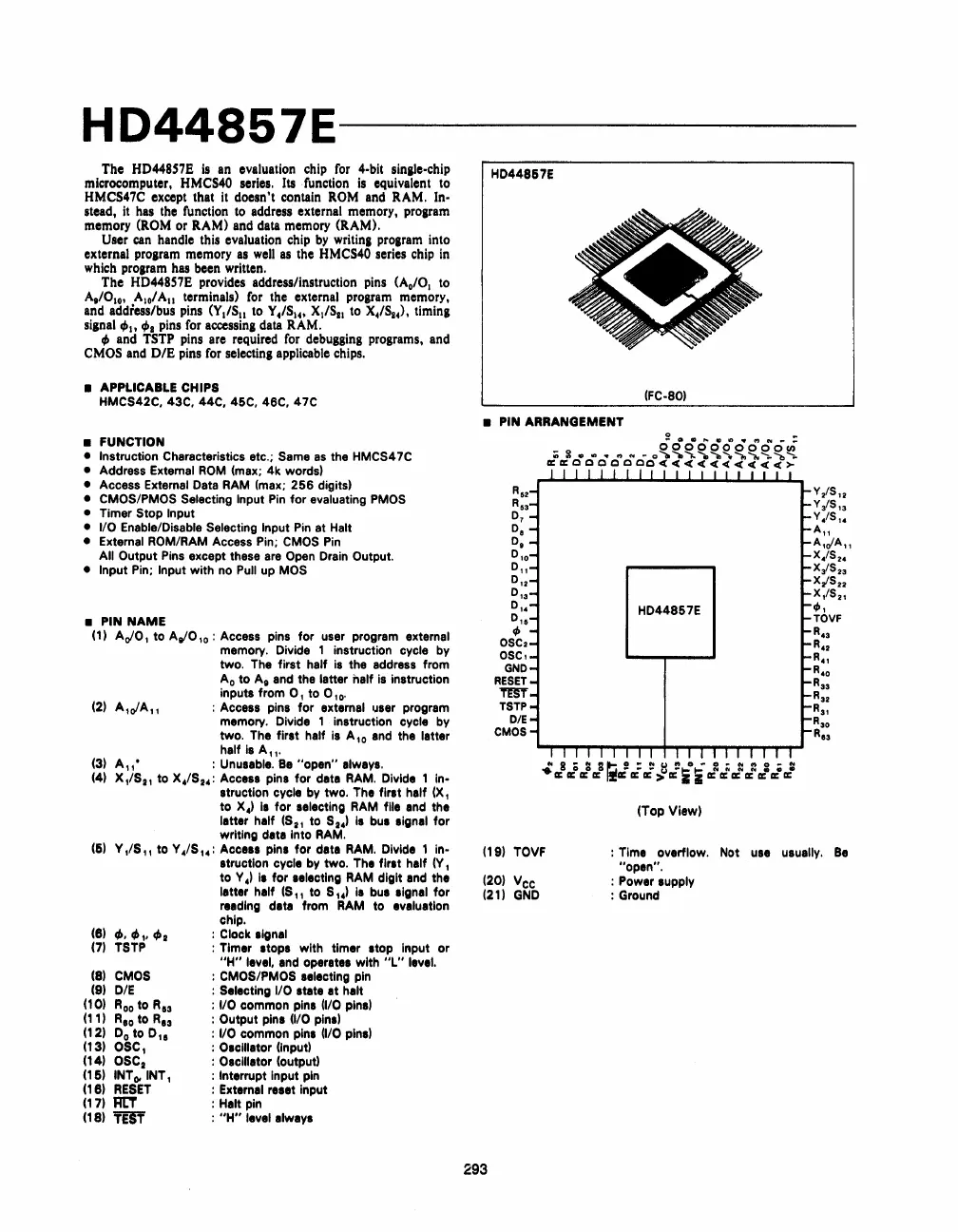
(FC-80)
• PIN
ARRANGEMENT
R52
R53
0
7
De
De
0'0
0"
012
0'3
0'4
015
If>
OSC,
OSC,
GNO
RESET
m'f
TSTP
DIE
CMOS
(19) TOVF
(20)
Vee
(21)
GND
293
HD44857E
(Top
View)
: Time overflow. Not use usually. ee
"open".
: Power supply
: Ground


 To Next Page
 Loading...