EasyManua.ls Logo

Hitachi AP1 - Page 372

Hitachi AP1
378 pages
Print Icon
To Next Page IconTo Next Page
To Previous Page IconTo Previous Page
Loading...
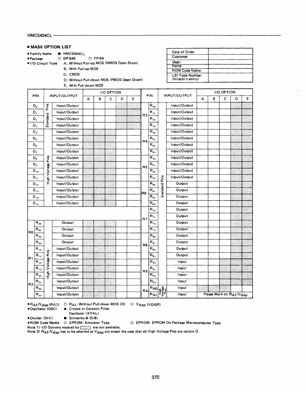
HMCS404CL------------------------------------------------------------------------
• MASK OPTION LIST
-
Family
Name
- Package
-
I/O
Circuit
Type
• HMCS404CL
o DP·64S 0 FP·64
A;
Without
Pull·up MOS (NMOS Open Drain)
B; With
Pull·up MOS
C; CMOS
0;
Without
Pull·down MOS (PMOS Open Drain)
E; With
Pull·down MOS
I/O
OPTION
PIN
INPUT/OUTPUT
A
B
C
o E
Do
~
Input/Output
I:»>L«<::
t---
a:
~"tl
Input/Output
I>::»[:>})}
~
t
Input/Output
I:::::}>t:::»>
0,
en
Input/Output
H>:::::d?L?::;-:
PIN
R,o
f--
R3
R3I
f--
Rll
f--
R"
R.
o
f--
R4
R"
f--
R'
2
~
Rso
I---
RSI
RS
~
I---
R
s
,
R.
o
f--
R6I
R6
f--
R'
2
~
R,o
f--
R7I
R7
~
~
R80
I---
R81
RS
I--
R82
I--
R
8
,
R.
o
I--
R"
R9
I---
R'
2
~
RA
RAO
Date
of
Order
Customer
Dept.
l'Ifame
ROM
Code Name
LSI
Type
Number
(Hitachi's
entry)
I/O
OPTION
INPUT/OUTPUT
A B C
0 E
Input/Output
L«::
I(:)}
Input/Output
mr\
tm~E
Input/Output
r>«
1:«<
Input/Output
I?Y:}
I\}}:
Input/Output
I<{:}
I»>:
Input/Output
:??>:
1:»>
Input/Output
2}?
f<>/
Input/Output
':S:::{:;
b}2
Input/Output
I<::)}
[/{:
Input/Output
1:/3/:
[\/t
Input/Output
::}})
?::::}
:}((:
«<
c:
Input/Output
a:
~
Output
;::::«;
;:::::;:::;:
"tl
Output
:\){:
~:>{<
~
en
Output
:<>:::::
I{«:
Output
v::»
1:<:)::
Output
[<:?~
I}{}
Output
k\{)
I:C}}
Output
:?}
i:\\}
Output
:«
I»>:
Output
I::?}{
[}/(
Output
[{{::::
[{\
Output
b:><
It<:?
Output
I:»>
k})
Input
):::::>
F:::);:::
F<t:
Input
:}{{
r>?>
k:«
Input
}:(::::
1\:\)
~t}/
Input
k{:}
L::))
tt<~::
'5,~~
Input
[%
I>~>r
IH!I+
~
:toQ:
Input
Please
Mark
on
RA1/Vdisp
>
-RA1/Vdisp(RA1)
0
RA1:
Without
Pull·down MOS (D) 0
Vdisp
(VDISP)
-Oscillator
(OSC) • Crystal
or
Ceramic
Filter
Oscillator
(XTAL)
-Divider
(DIV)
• Divide·by-S (D·S)
-ROM
Code Media 0 EPROM:
Emulator
Type 0 EPROM: EPROM On·Package
Microcomputer
Type
Note
1)
I/O
Options
masked
by
~
are
not
available.
Note
2)
RA1/Vdisp
has
to
be selected
as
Vdisp
pin
exept
the
case
that
all High Voltage Pins
are
option
D.
370