---------------------------------------------------------HMCS46C,HMCS46CL
•
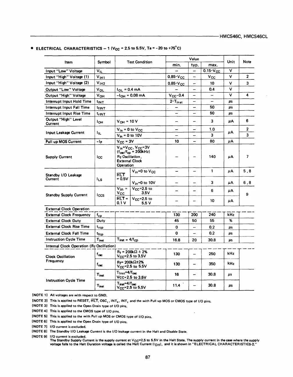
ELECTRICAL
CHARACTERISTICS
- 1
(Vee
=
2.5
to
5.5V,
Ta
=
-20
to
+75°C)
Item
Symbol
Test
Condition
min.
Value
typo
max.
Input
"Low"
Voltage
VIL
- -
0.15·Vce
Input
"High"
Voltage (1)
VIH1
0.S5-
V
ee
-
Vce
Input
"High"
Voltage (2)
VIH2
0.S5-
V
ee
-
10
Output
"Low"
Voltage
VOL
10L =
0.4mA
- -
0.4
Output
"High"
Voltage
VOH
-IOH =
O.OS
mA
Vee-
O
.4
-
-
Interrupt
Input
Hold
Time
tiNT
2'Tinst
-
-
Interrupt
Input
Fall
Time
tflNT
-
-
50
Interrupt
Input
Rise
Time
trlNT
- -
50
Output
"High"
Level
10H
VOH
=
10V
-
-
3
Current
Vin = 0
to
Vee
- -
1.0
Input
Leakage
Current
IlL
Vin
= 0
to
10V
-
-
3
Pull
up
MOS
Current
-Ip
Vee
=
3V
10
-
SO
Vin=Vee,
Vee=3V
(fose/fcp =
200kHz)
Supply
Current
Icc
Rf
Oscillation,
-
-
140
External Clock
Operation
Vin=O
to
Vec
- -
1
Standby
I/O Leakage HIT
Current
ILS
=0.5V
Vin=O
to
10V
- -
3
Vin
=
Vee=2.5
to
- - 6
Standby
Supply
Current
Ices
Vec
3.5V
RIT=
Vce=2.5
to
- -
10
0.1
V
5.5V
External Clock
Operation
----------
,-----
--------------
r-200--240-
External Clock
Frequency
fcp
130
External Clock
Duty
Duty
45
50
55
External Clock Rise
Time
t
rcp
0 -
0.2
External Clock Fall
Time
tfcp
0
-
0.2
Instruction
Cycle
Time
Tinst
Tinst =
4/fcp
16.S
20
30.S
Internal Clock
Operation
(Rf
Oscillation)
----------
----
At
=
20Okn±2%
- - -
----
;---
----
fose
130
-
250
Clock Oscillation
Vee=2.5
to
3.5V
Frequency
fose
Rt=
200kil±2%
130
350
Vee=2.5
to
5.5V
-
Tinst
Tlnst=4/f
ose
16
-
30.S
Vee=2.5
to
3.5V
Instruction
Cycle
Time
Tinst=4/fosc
Tinst
Vee=2.5
to
5.5V
11.4
-
30.S
(NOTE
1 I
All
voltages
are
with respect to
GND.
(NOTE
21
This
is
applied
to
RESET,
HLT,
ose.,
INTo, INT. and the with
Pull
up
MOS
or
CMOS
type of I/O pins.
(NOTE
31
This
is
applied
to
the Open Drain type of
I/O
pins.
(NOTE
41
This
is
applied
to
the
CMOS
type of
I/O
pins.
(NOTE
51
This
is
applied to the with
Pull
up
MOS
or
CMOS
type of
I/O
pins.
(NOTE
61
This
is
applied
to
the Open
Drain
type of I/O pins.
(NOTE
71
I/O current
is
excluded.
(NOTE
81
The Standby I/O Leakage Current
is
the I/O leakage current
in
the Halt and Disable State.
(NOTE
91
I/O current
is
excluded.
Unit Note
V
V 2
V 3
V
V
4
IlS
IlS
Ils
IlA
6
2
IlA
r---
3
IlA
IlA
7
IlA
5,S
IlA
6,S
IlA
9
IlA
---
---
kHz
%
IlS
IlS
IlS
,--
----
kHz
kHz
IlS
IlS
The Standby Supply Current
is
the supply current at VCC=2.5 to 5.5V
in
the Halt State. The supply current
in
the case where the supply
voltage falls
to
the Halt Duration voltage
is
called the Halt Current (lDHI, and it
is
shown
in
"ELECTRICAL CHARACTERISTICS-2."
87
 Loading...

