HMCS46C,HMCS46CL------------------------------------------------------
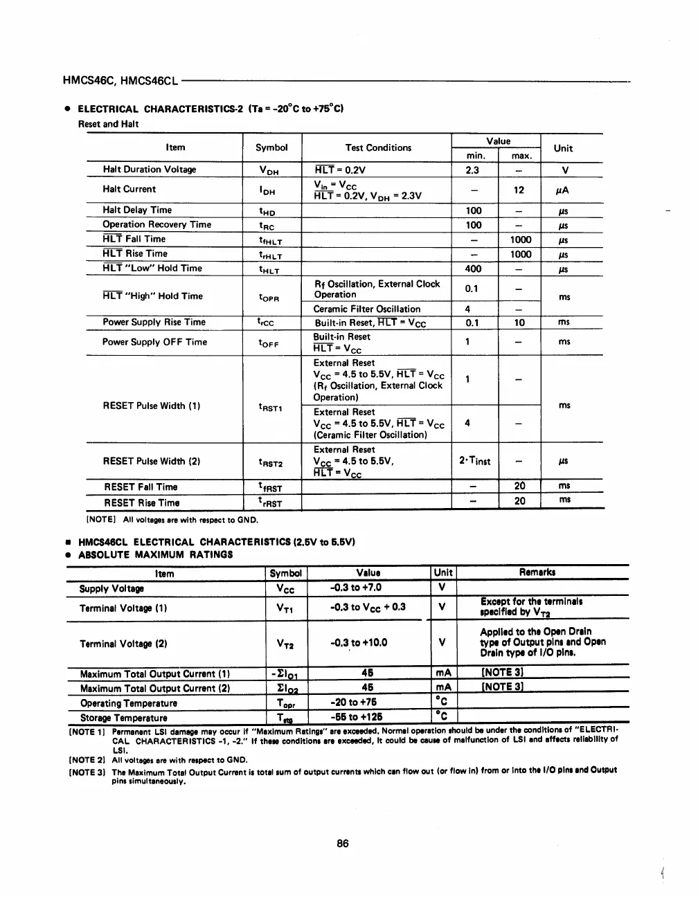
• ELECTRICAL CHARACTERISTICS-2
(Ta
= _20°C
to
+75°C)
Reset and
Halt
Item
Symbol
Test Conditions
Halt Duration Voltage
V
OH
HLT= 0.2V
Halt
Current
IOH
V
in
= Vee
HLT
= 0.2V, V
OH
= 2.3V
Halt Delay Time
tHO
Operation Recovery Time
t
Re
HLT
Fall
Time
tfHLT
HL
T
Rise
Time
trHLT
HLT
"Low"
Hold
Time
tHLT
Rf
Oscillation, External Clock
HL
T "High"
Hold
Time
tOPR
Operation
Ceramic
Filter Oscillation
Power Supply
Rise
Time tree
Built-in Reset,
H[T
= Vcc
Power
Supply OFF Time
tOFF
Built·in Reset
HLT=Vee
External Reset
Vee = 4.5
to
5.5V,
HLT
= Vee
(R
f
Oscillation, External Clock
RESET
Pulse
Width
(1)
Operation)
t
RSTt
External Reset
Vee = 4.5
to
5.5V,
HLT
= Vee
(Ceramic
Filter Oscillation)
External Reset
RESET
Pulse
Width
(2)
tRST2
Vee = 4.5
to
5.5V,
RLT= Vee
RESET
Fall
Time
t
fRST
RESET
Rise
Time
t
rRST
[NOTE)
All
voltages
ara
with
raspact
to
GND.
•
HMCS46CL
ELECTRICAL CHARACTERISTICS (2.6V
to
6.6V)
•
ABSOLUTE
MAXIMUM
RATINGS
Item
Symbol
Value
Unit
Supply Voltage
Vee
-0.3
to
+7.0
V
Terminal Voltage
(1)
V
T
,
-0.3
to
Vee + 0.3
V
Terminal Voltage
(2)
Vn
-0.3
to
+10.0
V
Maximum
Total Output Current
(1)
-tlo,
46
mA
Maximum
Total Output Current
(2)
tlo2
46
mA
Operating Temperature
Topr
-20
to
+76
°c
Storage Temperature
T_
-66
to
+126
°c
Value
Unit
min. max.
2.3
-
V
-
12
IlA
100
-
Ils
100 -
IJ.S
-
1000
IlS
-
1000
IJ.S
400
-
IJ.S
0.1
-
ms
4
-
0.1
10
ms
1 -
ms
1
-
ms
4
-
2·Tinst
-
Ils
-
20
ms
-
20
ms
Remarks
Except for the terminals
specified
by
V
T2
Applied
to
the Open
Drain
type of Output pins and Open
Drain type
of
1/0
pins.
[NOTE
3J
[NOTE 3]
(NOTE
1)
Permanant
LSI
demage
may
occur
If
"Maximum
Ratings"
areexcaeded.
Normal
operation
should
be
under
the
conditions
of
"ELECTRI·
CAL
CHARACTERISTICS
-1.
-2."
If
the.
conditions
ere
exceeded,
It
could
be
cause
of
malfunction
of
LSI
and
affects
reliability
of
LSI.
(NOTE
2)
All
voltages
ara
with
respect
to
GND.
(NOTE
3)
The
Maximum
Total
Output
Currant
is
total
sum
of
output
currants
which
cln
flow
out
(or
flow
In)
from
or
Into
the
1/0
pins
.nd
Output
pins
simultaneously.
86
 Loading...

