D-E99
Pin
Pin
Symbol
Function
No .
•
10
LINE MUTE • LINE amp final stage muting control
output
pin.
Outputs
Hi potential during
REC,
PLAY
and
REC-PAUSE
after recording
to
mute the
play signal
of
the LINE amp output.
Hi potential is
output
after
elapse
of
the
inhibit
time
of
120
ms during play, after elapse
of
the
inhibit
time
of
400
ms during record and
after
elapse
of
the
inhibit
time
of
1100
ms
when changing the mode from
FF
or
REW.
11
REW
SOL.
REW solenoid drive
output
pin.
Outputs
Lo
potential normally and Hi potential during
REC,
PLAY
and
REW.
--
-
-----------
12
FF
SOL.
FF
solenoid drive
output
pin.
Outputs
Lo
potential normally
and
outputs
Hi potential
I
during REC,
PLAY
and
FF.
'
13
PAUSE SOL.
i
· PAUSE solenoid drive
output
pin. Outputs·
Lo
potential normally and
outputs
Hi potential
I
during REC-PAUSE mode and
PLAY-PAUSE
mode.
I
-·---------------------~
•
14
NC
· Blank pin.
--------·---
15
RESET
I
· Initial reset
input pin.
This
pin input is set
to
Hi potential when power is supplied
to
perform initial resetting.
--
-----~
16
GND
· Connected
to
GND
---
--
--
17
osc 1
· The external resonance
circuit
is coupled
with
these
pins
to
operate the
built-in
clock
•
18
osc 2
oscillation circuit which is the
reference
of
microprocessor
operation. The oscillat1on
frequency is set
to
400 kHz.
-
-------------------·---
19
HALT
·HALT
pin. This pin changes from
Lo
potential
to
Hi
potential when power is supplied
I
and the program
of
the
microprocessor is executed.
It
is
set
to
Lo potential when povier
is set
to
OFF
and the execution
of
the program
stops
and is held.
-~
20
TEST
• Microprocessor test pin. Connected to Vee pin @ because
this
is
not
used.
•
21
Vee
• Power pin. Applies
+5V.
-
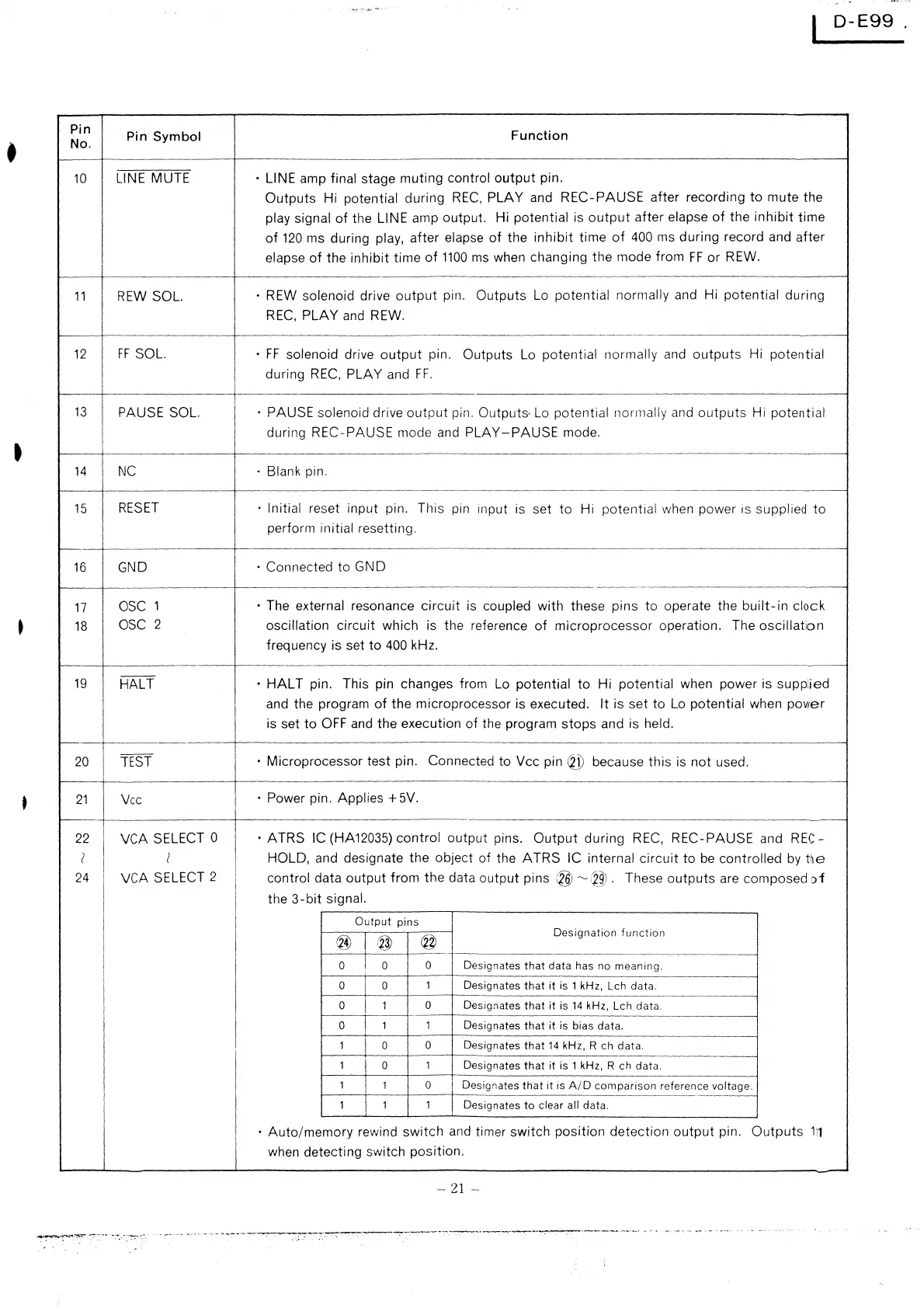
22
VCA SELECT 0
•
A TRS IC
(HA
12035)
control
output
pins.
Output
during
REC,
REC-PAUSE
and REC-
I I
HOLD, and designate the object of the
ATRS
IC internal
circuit
to
be
controlled
by
t~e
24
VCA SELECT 2 control data
output
from
the
data
output
pins
.~~~~'·
These
outputs
are composed
Df
the
3-bit
signal.
Output
pins
@
@
®
Designation
function
I
0
i
0
--------
0
Designates
that
data
has
no
meaning.
0
I
0
1
Designates
that
it
is 1 kHz, Leh
data.
--
0
I
1
0
Designates
that
it
is
14
kHz, Leh data.
I
0
I
1
1
Designates
that
it
is
bias
data.
·-----------
1
0
0
Designates
that
14
kHz, R eh
data.
--
1
0
1
Designates
that
it
is 1 kHz, R eh
data.
1 1 0
Designates
that
1t
is
AID
comparison
reference
voltage.
I
1 1
1
Designates
to
clear
all
data.
I
·
Auto/memory
rewind
switch
and timer
switch
position
detection
output
pin.
Outputs
1'1
when detecting switch position.
-
21
-
------.-...--
..
-----------<~----
-----
---~----~-----
-----~~.
 Loading...