Section
VIIl THEORY OF OPERATION Model 3455A
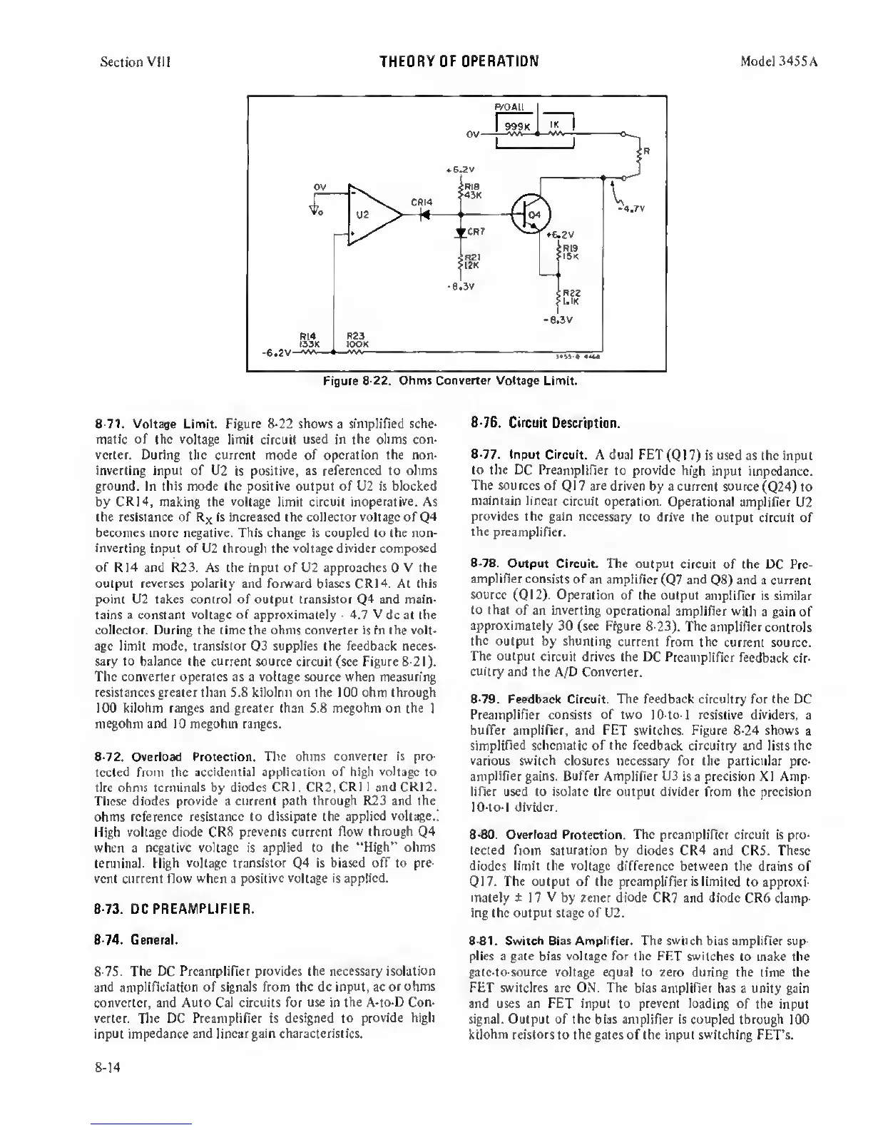
8-71. Voltage
Limit. Figure
8-22 shows
a
simplified
sche-
matic of the voltage
limit circuit
used in the ohms con-
verter. During the current mode of operation the non-
inverting input of U2
is
positive, as referenced to ohms
ground.
In this mode the positive output of U2 is blocked
by CRM, making the
voltage
limit circuit
inoperative.
As
the resistance of
Rx
is increased the coUector voltage of
Q4
becomes more negative. This change is coupled to the non-
inverting
input of U2 through the
voltage divider
composed
of RI4 and R23. As the input of U2 approaches
0
V the
output reverses polarity and forward biases CR14.
At
this
point U2 takes control of output transistor Q4 and main-
tains a constant
voltage
of approximately
-
4.7 V dc at the
collector. During the time the ohms converter
is in
the volt-
age limit mode, transistor
Q3
supplies the feedback neces-
sary to balance the
current
source
circuit (see Figure 8-21).
The converter operates as
a
voltage source when measuring
resistances greater than S.8 kilohm on the 100 ohm through
100 kilohm ranges and greater than 5.8 megohm on the
1
megohm and 10 megohm ranges.
8-72.
Overload Protection. The ohms
converter is pro-
tected
from the accidential application of high
voltage
to
the ohms terminals by diodes (TRl. CR2.
CRl 1 and CR12.
These diodes
provide
a
current path through R23 and the
ohms
reference resistance to dissipate the applied
voltage.
High voltage diode CR8 prevents current
flow through
Q4
when
a
negative
voltage is
applied to the “High" ohms
terminal.
High voltage transistor
Q4
is biased ofT to pre-
vent current flow when a
positive voltage
is
applied.
8-73.
DC PREAMPLIFIER.
8-74.
General.
8-75. The DC Preamplifier provides the necessary isolation
and amplifidation of signals from the dc
input,
ac or
ohms
converter, and Auto Cal circuits for use in
the A-to-D Con-
verter. The DC Preamplifier is designed to
provide high
input impedance and
linear gain characteristics.
8-76. Circuit
Description.
8-77. Input Circuit.
A dual FET(Q17)
is used as the input
to the DC Preamplifier
to provide high
input impedance.
The sources of
Q17
are driven
by a current source
(Q24)
to
maintain linear
circuit operation.
Operational amplifier
U2
provides
the gain necessary
to drive the
output circuit of
the
preamplifier.
8-78.
Output
Circuit.
The output
circuit of the DC Pre-
amplifier consists
of an amplifier
(Q7
and
Q8)
and
a
current
source
(QI2). Operation
of the output
amplifier is similar
to that
of an
inverting
operational
amplifier
with a gain of
approximately
30
(see Figure 8-23).
The amplifier
controls
the output by shunting
current from the
current source.
The output
circuit drives the DC
Preamplifier feedback
cir-
cuitry and the A/D Converter.
8-79.
Feedback Circuit. The feedback circuitry for the DC
Preamplifier
consists of two
10-tu-l
resistive
dividers, a
bulTer amplifier, and FET switches. Figure 8-24 shows
a
simplified
schematic
of
the feedback
circuitry and lists the
various switch closures necessary for the particular pre-
amplifier
gains.
Buffer
Amplifier
U3
is a precision XI Amp-
lifier used to isolate the output divider from
the
precision
10-to-l
divider.
8-80.
Overload Protection. The preamplifier
circuit is pro-
tected from saturation
by diodes CR4 and CRS. These
diodes limit the voltage
difference
between
the drains of
Q17. The output of the preamplifier is limited
to approxi-
mately
t
17
V
by Zener
diode
CR7 and diode CR6
clamp-
ing the output stage of U2.
8-81. Switch
Bias Amplifier.
The switch
bias amplifier sup-
plies
a
gate bias voltage for the FF.T
switches to make the
gate-to-source voltage equal to zero
during the time the
FtT switches are ON. The bias amplifier
has a unity gain
and uses an FET input to prevent loading of the
input
signal. Output of the bias amplifier is coupled through
100
kilohm reistors
to the gates of the input switching FET's.
8-14
 Loading...