'"
" :(
,
~:'
, "
;1' 1,
,', ,
I,
, I
" "
.,.1
',1,;":,
,;'",
,
ill,
"I
"
" '
,;/
• j '. '
I,'"
j\
:'l'
,I '"
"~I
.1 '
,
ponenti~l~~rve.
Ifa
c~nstant
vC?ltage"ls~aintained,'
",'.
',.a
,I'
the
attenuation
rises
.with
increasing temperature.
'.
"
"'1
1
"With
a'
constant
current,
,the atten:uation"
drops!
'" ,I , : '
with
increasing temperature. The fact.
that
theat-
'i '
/.",
" tenuation varies oppositely ,with temperature
for
constant-voltage and vconstant-current operation
suggests
that
an
optimum
voltage
with
aselected
series resistor added between
the
..ource and
the
PIN
Modulatorwould
give
temperatu~ecomp'etisa~
tion
over
,a'
liInited;\;,H~rating
range. This compensa-
tion
is
not
built
into
the
PIN Modulator,
2.a
3.0
, '
1 '
" ,
" '"
, ,';'
, , ,
1,1
I
I"
,
'.I
) 'I I
.:
,,r
, "
, i
1.8,
2:0
2.4'
,FRE'QUENCY
(GHz)
, ,
, ,
.
()
o.a',
" '
1.2
,
"
!
",',
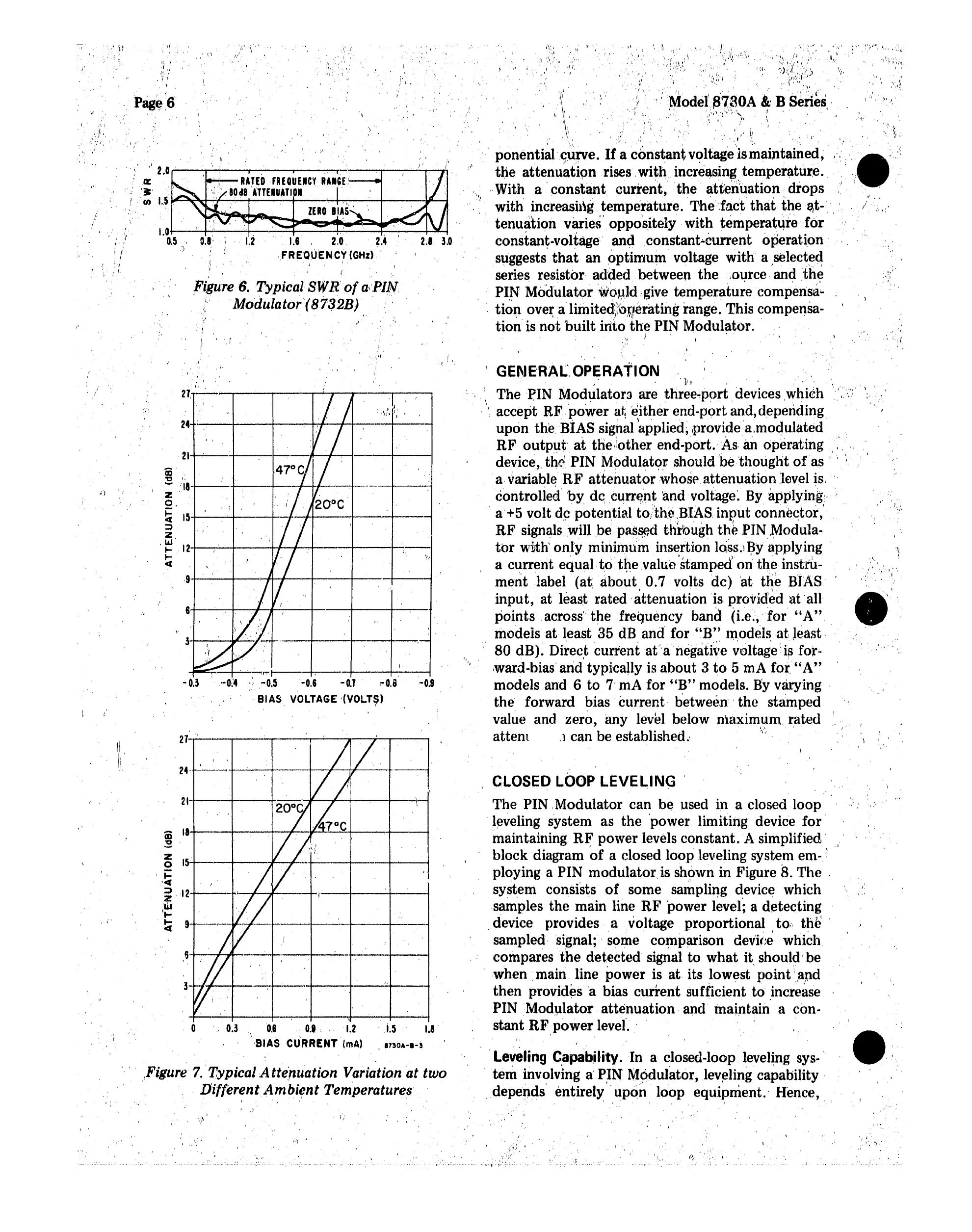
Fi,gu're
6. Typical 8WR'of
a,'PIN
, " Modulator(87a2B) '
,',
,I
,I
, '
LO+---~H"_-~---+__-,__+----+_
_+~
0.5
('j -I
,I"
.\(/
"
1
,
,P8g~',6'
"
, 'I
, ,
, ,
,I
ti
I_~'
':
"2.0
,.---r---j---,.---r-----:-:-r
, ,II:
,:'~'
"
I (J)
1.,5
iIl"',
~~""f__
+__-_+---'--+:-:--.,._._f----__It'"___i
;' "
! \' '
I I
1
,
I '\
/,f.
1,1,'
,
,I,
1
I,'
, ,I
CLOSED
LOOP
LEVELING'
The PIN,Modulator can be used
i.n
a closed loop
leveling system as
the
'power limiting device
for'
maintaining
RF
power levels constant. A
simplified',
block diagram 'of a closed loop leveling system em- i
ployinga
PIN modulator,is shown in Figure
8.
The
.
system consists
of
some sampling device which
samples
the
main line RF. power level: a detecting
,device .provides a voltage proportional I to.
th~
.
sampledvslgnak some comparison device which
compares
the
detected signal
to
what
it
should'
he
when main line power is
at
its lowest 'point:',apd
then
provides 'a bias
current
sufficient
to
Increase
PINl\'lod\llator
attenuation and maintain a con-
stant
R}'power
level. .
'Leveling
Capab.il·ity.
In
a closed-loop leveling sys-'
tern. involving a
P~N'
Modulator, Ieveling capability
.depends entirely
'upon
loop
equipment.' Hence,
\.
GEI\JERAL'.
OPERATION
J '1'"
I"~
" ,
,
'I'hePtN
Modulators are three-port.devices ,whieh";,'':',:'
'"
." accept RF
power
~G
e,ither end-port and, depending
upon
the. BIAS signal applied, provide a.modulated
RF
output'
at
the
,,'other end-port.
'As,
an operating
,"
device"
the;
PINM'odulat<;>~
should
be
'thought
ofas
:
.a,
variableRF
attenuator
whose
attenuationlevel
is,
.,
controlled
by
decurrent
and
voltage. By applyinrt", .
,
a+5
volt de potential to/the,;BIAS
inI;>ut
connector,
.
RF
signals will
be
passed through
the
PIN)\1odula-
tor
with'
only
minimum insertion loss;By applying
a current equal
to
the-value'stamped
on'
the
instru-
ment
label
(at,
about
0.7
volts de) 'at
the
BIAS
),
'~
"
input,
at least rated 'attenuation
IS
provided
atall
points.
across'
the
frequency band (i.e.,' for
"A"
models
at
least '35 dB
and
for
"B"
modelsat
least
80
dB)~
Direct
cUITentat"a'neg~ti~'e~oltag'e'
is'
foro.
"'I'
ward-bias' arid typically is
about
3
to
5 rnA for,
"A"
models and 6
to
7' mA for
"B"
models. By
varying·
the
forward bias
current
between'
the
stamped
value and zero, any level below maximum rated
attern
.1
can be established.
!\'j'
-0.9
, I
--+
..........
.....,,..,.,~,
---+,....---+---+-----1
-
0.3
"-0~4
,.',-0.5
-0.6
-
OJ
,..
0.8
,
~'
I
BIAS
VOLTAGE
'(VOLT~)
21-,t--+----1"
24
-+-.;...
......
-t----t---J'--:Ir--~,t---_t
6i+--+...,.q.-
,,---+---+-~.t----+---i
,0
',0.30.8
0.'"
,,1.2
,i.5
I.a
'
·BIAS
CU'RRENT
(mA)
1130A-I-;
iii
181-t---t--.,._._f---:.f'7-·¥-''-''-=-t----,-t----i
'0,
--
~
151'1"
--+-----I--#--+--+_._
.-t-----1
'
...
'~
;:)
12·+----1-'--r--:tf--
,m
'
...
~
9-t--~.._,..__t--+--,_+_-_+--.;
I
I'
\,
'
~)
, ,
',"
Figure
7.
Typica'l
Attenuation
Variation
'at
two
, D'ifferentAmbii!nt Temperatures'
, '
;'
, /
",
I
, "
,,',
.
I'
,"',
~
.:
_",I
 Loading...