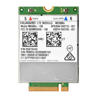
Please note that the differences of PCB pad among 30 mm × 30 mm LGA modules.
The pin 49, pin 53 and pin 57 of MU709, ME209u-526, ME909u-523 and
ME909s/MU509-65 are empty.
The pad size and function of the antenna interface among 30 mm × 30 mm LGA
modules are different, see Table 2-12 .
3.2.2 Requirements on PCB Layout
To reduce deformation, a thickness of at least 1.0 mm is recommended.
Other devices must be located more than 3 mm (5 mm recommended) away
from the two parallel sides of the LGA module (rework requirement),and other
sides with 0.6 mm. The minimum distance between the LGA module and the
PCB edge is 0.3 mm.
When the PCB layout is double sided, the module must be placed on the second
side for assembly; so as to avoid module dropped from PCB or component
(located in module) re-melding defects caused by uneven weight.
Figure 3-3 PCB Layout (unit: mm)
3.3 Assembly Processes
3.3.1 General Description of Assembly Processes
Tray modules are required at SMT lines, because 30 mm × 30 mm LGA modules
are placed on ESD pallets.
Reflow ovens with at least seven temperature zones are recommended, the
reflow profile please refer to Figure 3-5 .

 Loading...


