Appendix B. System Address Maps
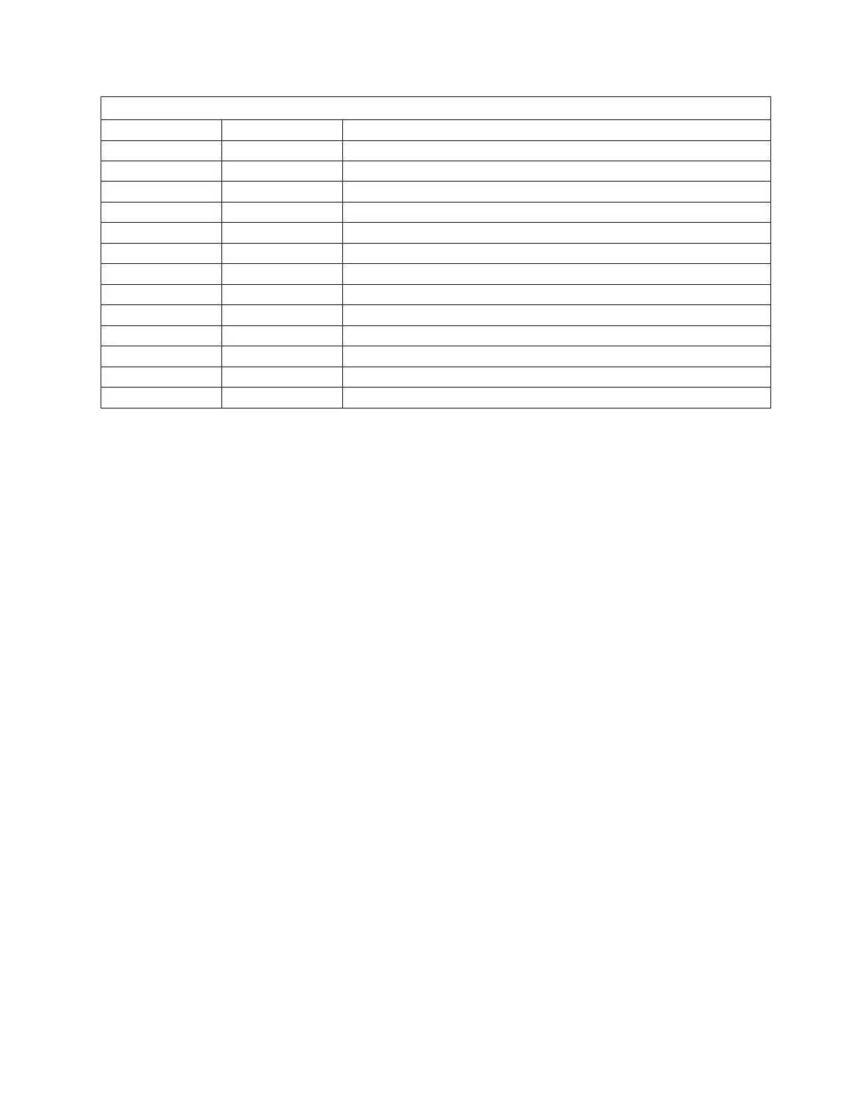
Table 51 (Page 2 of 2). Input/Output Address Map
Address (Hex) Size (Dec) Description
0378–037F 8 bytes LPT2
03BC–03BE 4 bytes LPT1 (system board)
03E8–03EF 8 bytes COM3 or COM4
03F0–03F5 6 bytes Floppy channel 0
03F6 1 byte IDE channel 0
03F7, bit 7 1 bit Floppy disk change
03F7, bits 6:0 7 bits IDE status channel 0
03F8–03FF 8 bytes COM1 (system board)
04D0 1 byte Interrupt edge/level control 1
04D1 1 byte Interrupt edge/level control 2
0CF8–0CFB 4 bytes PCI configuration address register
0CF9 1 byte Reset control register
0CFC–0CFF 4 bytes PCI configuration data register
Appendix B. System Address Maps 55
 Loading...