

N
nicholas59Jul 26, 2025
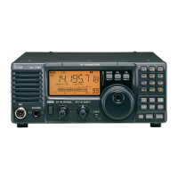
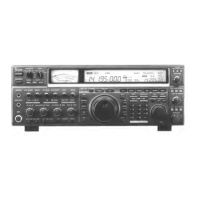
How to fix Icom IC-746 when power does not come on?
- MMadison Lane MDJul 26, 2025
If your Icom Transceiver does not power on when you push the [POWER] switch, the issue may be due to the DC power cable being improperly connected, a blown fuse, or a depleted battery (if using a 12V battery). Reconnect the power cable correctly. Check the fuse and replace it if necessary. There are two fuse locations: one in the DC power cable and another in the PA unit. If using a battery, check its voltage with the [POWER] switch pushed IN.