4 - 4
The lock voltage is also used for the receiver tunable band-
pass filters to match the filter’s center frequency to the
desired receive frequency. The lock voltage is amplified at
the buffer amplifier (Q29) and is then applied to the band-
pass filters (D7, D9–D11).
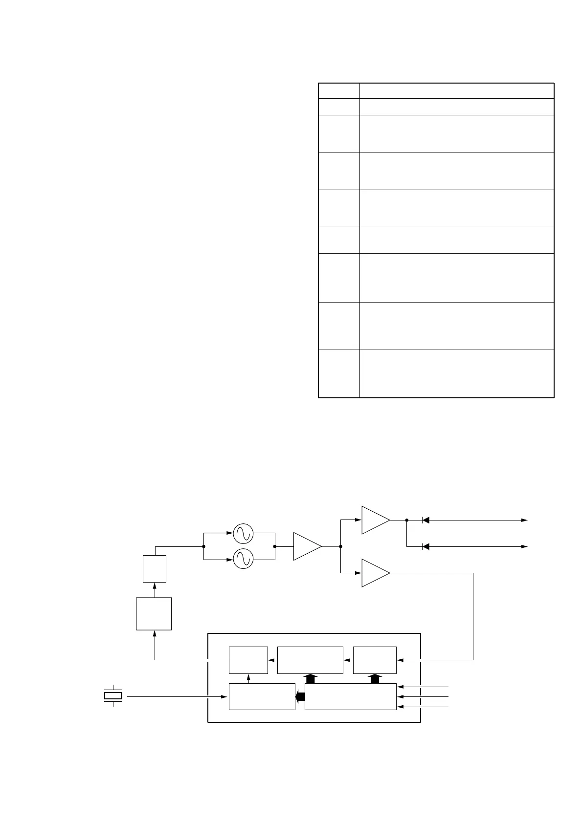
4-3-2 VCO CIRCUIT
The VCO circuit contains a separate Rx VCO (Q21, D19,
D20, D40, D41) and Tx VCO (Q23, D21, D22, D42, D43).
The oscillated signal is amplified at the buffer amplifiers
(Q19, Q20) and is then applied to the Tx/Rx switch (D17,
D18). Then the receive 1st LO (Rx) signal is applied to the
1st mixer (Q2) via the amplifier (Q3) and the transmit (Tx)
signal to the driver (Q17).
A portion of the signal from the buffer amplifier (Q19) is fed
back to the PLL IC (IC12, pin 11) via the buffer amplifier
(Q18) as the comparison signal.
LINE
HV
VCC
CPU5V
+5V
+8V
R8V
T8V
MT8V
DESCRIPTION
The voltage from the external power connector.
Same voltage as the HV line passed through the
power control circuit (Q12) controlled by PWON
signal from the CPU (IC20, pin 77).
Common 5 V converted from the HV line at the
5V regulator circuit (IC17). This voltage is sup-
plied to the CPU regardless of the power switch.
Common 5 V converted from the VCC line at the
+5V regulator circuit (Q42, Q43, D30) using the
CPU5V line voltage as the reference.
Common 8 V converted from the VCC line at the
+8V regulator circuit (IC16).
Receive 8 V converted from the VCC line at the
R8V regulator circuit (Q36, D27) using the +8V
line voltage as the reference and controlled by
VRX signal from the CPU (IC20, pin 76).
Transmit 8 V converted from the VCC line at the
T8V regulator circuit (Q40, D29) using the +8V
line voltage as the reference and controlled by
VTX signal from the the CPU (IC20, pin 75).
Transmit 8 V converted from the VCC line at the
MT8V regulator circuit (Q38, D28) using the +8V
line voltage as the reference and controlled by
TMUT signal from the the CPU (IC20, pin 62).
4-4 POWER SUPPLY CIRCUIT
VOLTAGE LINE
 Loading...