WARNING! The IM483 Driver components are sensitive to
Electrostatic Discharge (ESD). All handling should be done at
an ESD protected workstation.
WARNING! Hazardous Voltage Levels may be present if you
are using an open frame power supply to power the IM483
Driver.
WARNING! Ensure that the Power Supply output voltage does
not exceed the maximum input voltage of the IM483 Driver.
WARNING! Do not operate the IM483 Driver without a Cur-
rent Adjustment Resistor!
A resistor MUST be placed between the Current Adjust Input
(Pin 2 on P2) and ground (Pin 3 on P2) to keep the IM483
Driver and/or motor in a safe operating range.
© Intelligent Motion Systems, Inc.
For More In for ma tion:
See the com plete IM483 Product Manual
on the IMS Product CD or at www.imshome.com
Rev. 062105
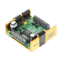
IM483
HIGH PERFORMANCE MICROSTEPPING DRIVER
M483 Quick Reference And Installation Guide
The primary function of IM483 Quick Reference and Installation
Guide is to acquaint the user with the specifi cations, basic wiring
and confi guration of the IM483 Microstepping Driver. The full prod-
uct manual is available in Acrobat PDF format on the IMS Product
CD, shipped with the product. It also may be downloaded from the
IMS web site at http://www.imshome.com.
Notes And Warnings
Please observe the following when handling, connecting and using
your IM483 driver. Failure to observe these points may result in
damage to the drive. All warranty and disclaimer information is
located in the full product manual on the CD and should be refer-
enced for more information.
Electrical Specifications
Input Voltage .............................................. +12 to +48 VDC
Phase Output Current (RMS) ........................................... 3A
Phase Output Current (Peak).................................. 0.4 to 4A
Quiescent Current
Inputs/Outputs Floating .................................. 70mA Typ.
Active Power Dissipation (I
OUT
=3A RMS) ......................... 12W
Thermal Specifications
Ambient Temperature ......................................... 0° to 50° C
Storage Temperature..................................... -40° to 125° C
Max. Plate Temperature.............................................. 70° C
Recommended Power Supplies
IP404 Unregulated Linear Supply
Range
Input 120 VAC Version ....................................... 102-132 VAC
240 VAC Version ....................................... 204-264 VAC
No Load Output Voltage* ................................43 VDC @ 0 Amps
Continuous Output Rating*..............................32 VDC @ 2 Amps
Peak Output Rating* ......................................26 VDC @ 4 Amps
ISP200-4 Unregulated Switching Supply
Range
Input 120 VAC Version ....................................... 102-132 VAC
240 VAC Version ....................................... 204-264 VAC
No Load Output Voltage* ................................41 VDC @ 0 Amps
Continuous Output Rating*...........................38 VDC @ 1.5 Amps
Peak Output Rating* ......................................35 VDC @ 3 Amps
* Measurements taken at 25°C, 120 VAC, 60 Hz.
Mechanical Specifications
Dimensions in Inches (mm)
1
2
3
4
5
6
7
8
0.150
(3.8)
2.45
(62.23)
2.750
(69.9)
1.00
(25.4)
0.312
(7.92)
0.290
(7.4)
2.710
(68.8)
3.00
(76.2)
0.030
(0.8)
4X Ø 0.160
(4X Ø 4.1)
1.20
(30.50)
0.410
(10.4)
1734
1
0.025
(0.6)
18
IM483-34P1
Optically Isolated Inputs
+5VDC Optocoupler Supply P1:4
Step Clock P1:2
(10 MHz max. Freq.)
CW/CCW Direction P1:3
Enable/Disable P1:5
Reset P1:6
470 Ω
HCP0630
Current Limiting Resistor Values
+VDC
5
10
12
15 24
–
681
1000
1300
2670
R
LIMIT
Controller
Output
IM483 Input
R
LIMIT
*
1/4 W 1%
Open Collector Interface
+5 VDC
Controller
Output
Opto Supply P1:4
IM483 Input
TTL Interface
* WARNING! An R
LIMIT
Current Limiting Resistor is required when the Opto Supply
Voltage is greater than +5VDC.
8 Pin #
34 Pin #
Pin Name Function
3 Resolution Select 3
Microstep Resolution Select 3 Input.
2
4
Step Clock Input
A positive going edge on this input advances the motor
one increment. The size of the increment is dependent
upon the settings of the resolution select switch SW1.
3
6
Direction Input
This input is used to change the direction of the motor.
Physical direction also depends upon the connection of
the motor windings.
4
8
Opto Supply
This +5 VDC input is used to supply power to the
isolated logic inputs. A higher voltage may be used, but
care must be taken to limit the current through the
opto-coupler.
5
10
Enable/Disable
This input is used to enable/disable the output section
of the driver. When in a Logic HIGH state (open), the
outputs are enabled. However, this input does not
inhibit the step clock, therefore, the outputs will update
by the number of clock pulses (if any) applied to the
driver while it was disabled.
6
12
Reset Input
When LOW, this input will reset the driver (phase
outputs will disable). When released, the driver will be
at its initial state (Phase A OFF, Phase B ON).
7
14
Fault Output
This output indicates that a short circuit condition has
occurred. This output is active LOW.
8
16, 26
On-Full-Step Output
This open collector output indicates when the driver is
positioned at full step. This output can be used to
count the number of full steps the motor has moved,
regardless of the number of microsteps in between.
This output is active LOW.
21 Step Clock Output
Non-isolated step clock output follows step input.
22 Direction Output
Non-isolated direction output follows direction input.
23 Resolution Select 0
Microstep Resolution Select 0 input.
24 Resolution Select 2 Microstep Resolution Select 2 input.
25
Resolution Select 1
Microstep Resolution Select 1 input.
27
Ground
Non-isolated ground. Common with power ground.
Connector P2
Pin # Pin Name
Function
1
Current
Reduction Adjust
Phase Current Reduction Adjustment Input. A resistor
connected between this pin and pin 2 will
proportionately reduce the current in both motor
windings approximately 0.5 seconds after the last
positive edge of the step clock input. The amount of
current reduced will depend upon the value of the
resistor used.
2
Current
Adjustment
Phase Current Adjustment. A resistor is connected
between this pin and P2:3 (GND) to adjust the
maximum phase current in the motor. A resistor
MUST be connected to this input or the IM483 WILL
latch into fault.
3
GND
Power Ground. The ground, or return, of the power
supply is connected here.
4
+V
Motor Supply Voltage. +12 to +48 VDC.
5
Phase B
Phase B of the stepping motor.
6
Phase B Phase B of the stepping motor.
7
Phase A
Phase A of the stepping motor.
8
Phase A
Phase A of the stepping motor.
—
—
——
Connector P1-8 And P1-34 Pin Assignments*