MEMORY INTERFACING
6.2.5
Bus
Control Logic
Bus
control logic
is
shown in Figure 6-4. The bus controller
is
implemented
in
two PALs.
One PAL
(PAL-l)
follows the 80386 bus cycles and generates the overall bus cycle timing.
The second PAL (PAL-2) generates most of the bus control signals. The equations for these
PALs are listed
in
Appendix A of this manual.
The bus controller decodes the 80386 status outputs
(W
/R#,
M/IO#,
and
D/C#)
and
activates a command signal for the type of bus cycle requested. The command signal corre-
sponds to the bus cycle types (described
in
Chapter 3)
as
follows:
• Memory data read and memory code read cycles generate the Memory Read Command
(MRDC#) output. MRDC# commands the selected memory device to output data.
•
I/O
read cycles generate the
I/O
Read Command (IORC#) output. IORC# commands
the selected
I/O
device to output data.
• Memory write cycles generate the Memory Write Command (MWTC#) output. MWTC#
commands the selected memory device to receive the data
on
the data bus.
•
I/O
write cycles generate the
I/O
Write Command (IOWC#) output. IOWC# commands
the selected
I/O
device to receive the data
on
the data bus.
• Interrupt-acknowledge cycles generate the Interrupt Acknowledge
(INT
A#) output, which
is
returned to the 8259A Interrupt Controller. The second
INTA
cycle commands the
8259A to place the interrupt vector
on
the bus.
Figure 6-5 shows the timings of bus control signals for various memory accesses.
The bus controller also controls the READY # input to the 80386 that ends each bus cycle.
The PAL-2 bus control
PAL
counts wait states and returns READY# after the number of
wait states required by the accessed device. The design of this portion of the bus controller
depends
on
the requirements of the system; relatively simple systems need
less
wait-state
logic than more complex systems. The basic interface described here uses a PAL device to
generate READY
#;
other designs may use counters
and/or
shift registers.
The bus controller generates one of two bus cycles depending
on
which memory
is
being
accessed. Two inputs to
PAL-l
(CSOWS and
CSIWS)
from the address decoder determine
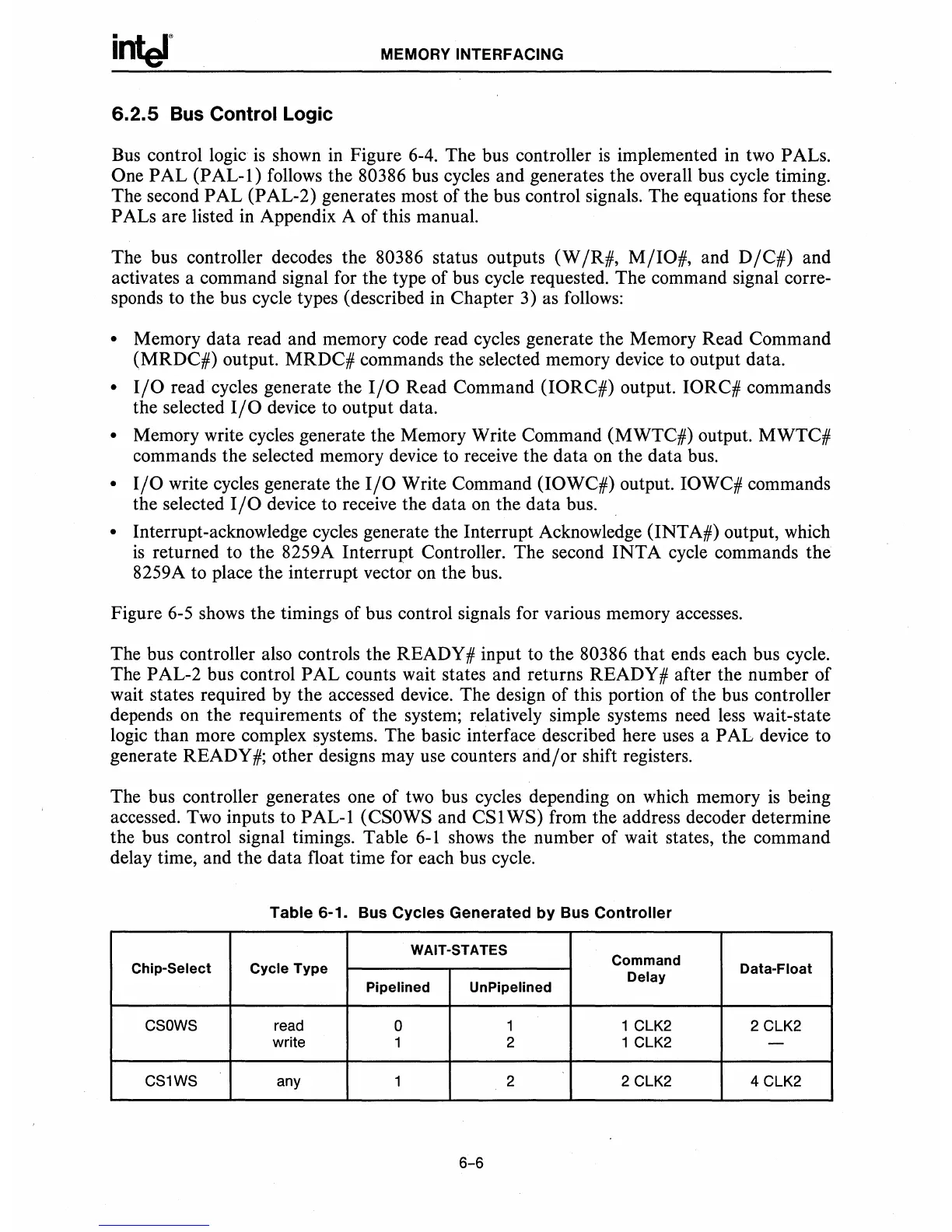
the bus control signal timings. Table
6-1
shows the number of wait states, the command
delay time, and the data float time for each bus cycle.
Table
6-1_
Bus
Cycles
Generated
by
Bus
Controller
WAIT-STATES
Command
Chip-Select
Cycle
Type
Delay
Data-Float
Pipelined UnPipelined
CSOWS
read
0 1
1 CLK2
2 CLK2
write
1 2 1 CLK2 -
CS1WS any
1
2 2 CLK2
4 CLK2
6-6
 Loading...


