Do you have a question about the JVC AV-2186ME and is the answer not in the manual?
Identifies critical safety components and emphasizes using recommended parts for safety.
Details conditions and specifies values for voltage and waveform measurements.
Explains part symbols and their corresponding values or types in circuit diagrams.
Defines indications for resistors, capacitors, and ground symbols in diagrams.
Highlights critical safety points regarding LIVE and ISOLATED GNDs during repair.
Overall block diagram for the first group of Color Television models.
Overall block diagram for the second group of Color Television models.
Circuit diagram for Main PWB, covering models AV-2186ME, AV-21MX56/S, AV-21MX76/G.
Continuation of Main PWB circuit diagram for AV-2186ME, AV-21MX56/S, AV-21MX76/G.
Circuit diagram for Main PWB, covering models AV-21MS16/H, AV-21MS26.
Continuation of Main PWB circuit diagram for AV-21MS16/H, AV-21MS26 models.
Circuit diagram for Main PWB, covering models AV-21MX16/G, AV-21MX16/S.
Continuation of Main PWB circuit diagram for AV-21MX16/G, AV-21MX16/S models.
Circuit diagram for the Bass PWB, including component layout and connections.
Illustrates the physical layout and traces of the Main PWB on the solder side.
Shows the physical layout and traces of the Bass PWB on the solder side.
Shows the physical layout and traces of the Bass PWB on the parts side.
Illustrates typical waveforms for various ICs and test points on the Main PWB.
Shows typical waveforms for critical test points on the CRT Socket PWB.
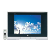
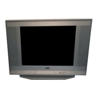
This document provides schematic diagrams and service information for a range of JVC Colour Televisions, including models AV-2186ME, AV-21MS16/H, AV-21MS26, AV-21MX16/G, AV-21MX16/S, AV-21MX56/S, and AV-21MX76/G. These televisions are designed for standard colour television reception and display, incorporating various features for video and audio processing.
The core function of these televisions revolves around receiving and processing broadcast signals or external video/audio inputs to display images and produce sound. The internal architecture, as detailed in the block diagrams, includes a tuner for receiving RF signals, a main microcomputer (IC701) that handles teletext decoding, IF-video processing, RGB signal processing, and synchronization. This central processing unit is crucial for managing the television's overall operation, including user input and display control. Video signals are processed through various stages, including SIF and VIF detection, AGC (Automatic Gain Control), AFT (Automatic Fine Tuning), and sound trap functions. Colour demodulation and RGB matrix processing ensure accurate colour reproduction. Synchronization separation (sync sep) and horizontal/vertical drive circuits are responsible for controlling the scanning of the CRT (Cathode Ray Tube) to form the image. Audio signals are processed through an audio select stage and amplified by an audio amplifier (IC601), with some models featuring an additional bass amplifier (IC671) for enhanced audio performance, indicated by the "MaxxBass®" branding.
Usage features are primarily controlled via the main microcomputer and external inputs. The televisions support multiple video input types, including S-Video, composite video (CVBS), and component video. This allows for connection to a variety of external devices such as DVD players, gaming consoles, and VCRs. Front-panel controls and a remote receiver enable user interaction for functions like volume adjustment, channel selection, and menu navigation. The OSD (On-Screen Display) and teletext decoder provide additional information and interactive features. Specific models may include PIP (Picture-In-Picture) control (IC301), allowing users to view multiple video sources simultaneously. The inclusion of a headphone jack and external speaker outputs offers flexible audio output options. The power supply section is designed to provide the necessary voltages for all internal components, with various regulators ensuring stable operation.
Maintenance features are primarily focused on safety and component replacement. The manual highlights "critical for safety" components, identified by a symbol and shading, emphasizing that these parts should only be replaced with manufacturer-recommended equivalents to ensure continued safe operation. This is a crucial aspect for service technicians. The document also provides detailed instructions for using the circuit diagrams, including explanations of part symbols, resistance and capacitance values, and voltage/waveform charts. These charts are essential for troubleshooting and verifying the correct operation of different circuit stages. A significant safety precaution is noted regarding the power circuit's ground differences (LIVE side GND and ISOLATED/NEUTRAL side GND). Technicians are explicitly warned not to touch these grounds simultaneously or short them, and to always disconnect the power cord before servicing, to prevent electric shock or damage to components. The circuit diagrams are presented as standard representations, with a note that actual circuit constants may change for improvement without prior notice. When ordering parts, technicians are advised to use the numbers appearing in the Parts List rather than those in the circuit diagram, as part numbers may differ due to performance improvements. The detailed breakdown of P.W.B (Printed Wiring Board) assembly names for different models helps in identifying the correct boards for replacement or repair. Semiconductor shapes are also provided for transistors and ICs, aiding in component identification and replacement.
| Screen Size | 21 inches |
|---|---|
| Display Technology | CRT |
| Aspect Ratio | 4:3 |
| Input/Output Connectors | RF, Composite Video, Audio |
| Inputs | RF |