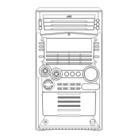
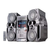
1-48 (No.22041)
4.8 ES3880F (IC104) : Video CD processor
• Pin Layout
• Block Diagram
• Pin function
1 ~ 25
75 ~ 51
50
26
~
76
100
~
Pin No. Symbol I/O Descriptions
1 VDD I 2.85V power supply.
2 RAS# O Memory row address strobe (active-low).
3 DWE# O Memory write enable (active-low).
4~12 MA[8:0] O Multiplexed memory row and column address.
13~28 DBUS[0:15] I/O Memory data.
29 RESET# I System reset (active-low)
30 VSS I Ground.
31 VDD I 2.85V power supply.
32~39 YUV[0:7] O B-bit YUV output.
40 VSYNC I/O Vertical sync; programmable for rising or falling edge.
41 HSYNC I/O Horizontal sync; programmable for rising or falling edge.
42 CPUCLK I RISC and system clock input.
43 PCLK2X I/O Doubled pixel clock I/O for screen video interface.
44 PCLK I/O 27-MHz pixel clock qualifier I/O for screen video interface.
45~49 AUX[0:7] I/O Auxillary control (AUX0 and AUX1 are open collectors).
50 VSS I Ground.
51 VDD I 2.85V power supply.
52~54 AUX[0:7] I/O Auxillary control (AUX0 and AUX1 are open collectors).
55~62 LD[0:7] I/O RISC interface data.
On-Screan
Display
32-Bit
RISC Processor
Gateway and
DMA Controller
Huffman
Decoder
Video
Processor
Transport
Parser
TDM
Interface
Serial Audio
Interface
8KB cache
CRT
Controller
DRAM
Interface
 Loading...