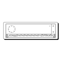
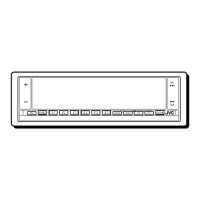
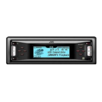
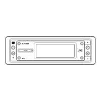
KD-LX330R/KD-LX110R
1-28
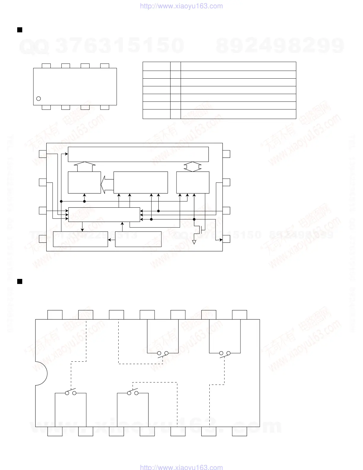
VCC WP SCL SDA
A0 A1 A2 GND
8 Vcc
7 WP
6 SCL
5 SDA
A0 1
A1 2
A2 3
GND 4
16kbit EEPROM allay
11bit
11bit
8bit
Address
decoder
Slave Ward
Address resister
Data
resister
START
STOP
ACK
Control circuit
High voltage osc circuit
Power supply
voltage det.
VCC
GND
A0,A1,A2
SCL
SDA
WP
-
-
I
I
I/O
I
Power supply.
GND
No use connect to GND.
Serial clock input.
Serial data I/O of slave and ward address.
Write protect terminal.
Symbol
I/O
Function
BR24C16F-X (IC703) : EEPROM
1. Pin layout
3. Block diagram
2. Pin function
14 13 12 11 810 9
1234 756
VDD C1 C4 I/O4 I/O3O/I4 O/I3
I/O1 O/I1 O/I2 I/O2 VssC2 C3
BU4066BCFV-X (IC322) : Quad analog switch
1. Pin layout & Block diagram
w
w
w
.
x
i
a
o
y
u
1
6
3
.
c
o
m
Q
Q
3
7
6
3
1
5
1
5
0
9
9
2
8
9
4
2
9
8
T
E
L
1
3
9
4
2
2
9
6
5
1
3
9
9
2
8
9
4
2
9
8
0
5
1
5
1
3
6
7
3
Q
Q
TEL 13942296513 QQ 376315150 892498299
TEL 13942296513 QQ 376315150 892498299
http://www.xiaoyu163.com
http://www.xiaoyu163.com
 Loading...