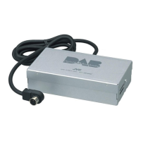
KT-DB1000
4
SECTION 3
Description of major ICs
3.1 MN102H60KCB (IC701) : Controller
• Pin layout
• Pin functions
No. Symbol I/O Function
1 - - Not use
2 LCDRS O Resistor select output terminal for LCD module
3 LCDR/W O Read/Write select output terminal for LCD module
4 LCDE O Data read/write start up output for LCD module
5~12 LCDDB0~7 O Data bus output 0 terminal for LCD module
13 JBUSCK I/O JBUS clock input/output terminal
14 JBUSDAI I JBUS data input terminal
15 JBUSDAO O JBUS data output terminal
16 JBUSI/O O JBUS input/output select output terminal
17 VDD - Powersupply terminal
18 SYSCKO O System clock(19.6608MHz) output terminal
19 GND - Connect to GND
20 XI I Connect to GND
21 NC O Open
22 VDD - Power supply trerminal
23 OSCI I X'tal connect terminal(19.6608MHz)
24 OSCO O X'tal connect terminal(19.6608MHz)
25 MODE I Mode setting input terminalpull up(single chip mode)
26 EEPRMDI I EEPROM(for preset data save)data input terminal
27 EEPRMDO O EEPROM(for preset data save)data output terminal
28 EEPRMCK O EEPROM(for preset data save)clock output terminal
29 EEPRMCS O EEPROM(for preset data save)chip select terminal
30~32 - - Not use
33 CKSEL O SYSCK output enable select terminal, "H" output enable
34 AVDD - Analogue power supply terminal
35 DAISEL O DAI output enable select terminal, "H" output enable
36 RDISEL O RDI output enable select terminal, "H" output enable
37 CIRSEL I CIR monitor output enable select terminal, "H" output enable
38 AGCSEL I AGC internal/external select terminal, "H" external(AGC outpput enable)
39 OPMODE0 I Operation mode setting terminal 0
40 OPMODE1 I Operation mode setting terminal 1
41 DUMMY I Dummy mode select terminal, "H" dummy mode
42 - - Not use
43 VREF- - Analogue reference power supply terminal, connect to GND
44 KEY0 I Test key analogue voltage onput 0
45 KEY1 I Test key analogue voltage input 1
46 KEY2 I Test key analogue voltage input 2
47 KEY3 I Test key analogue voltaeg input 3
48 TUSDA O Tuner PLL data output terminal
49 TUSCL O Tuner PLL clock output terminal
50 MPUCK O DAB MPU interface clock output terminal
51 MPUDAI I DAB MPU interface data input terminal
52 MPUDAO O DAB MPU interface data outut terminal
53 DABRST O DAB LSI/TUNER reset output terminal, "L" reset
54 VREF+ - Analogue reference poser supply terminal, connect to AVDD
55 DABDARX I FIC packet data stream output data input terminal
w
w
w
.
x
i
a
o
y
u
1
6
3
.
c
o
m
Q
Q
3
7
6
3
1
5
1
5
0
9
9
2
8
9
4
2
9
8
T
E
L
1
3
9
4
2
2
9
6
5
1
3
9
9
2
8
9
4
2
9
8
0
5
1
5
1
3
6
7
3
Q
Q
TEL 13942296513 QQ 376315150 892498299
TEL 13942296513 QQ 376315150 892498299
http://www.xiaoyu163.com
http://www.xiaoyu163.com
 Loading...