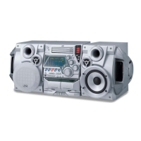
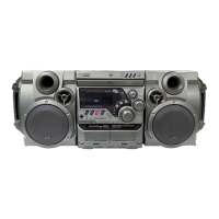
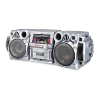
MX-GT700
1-33
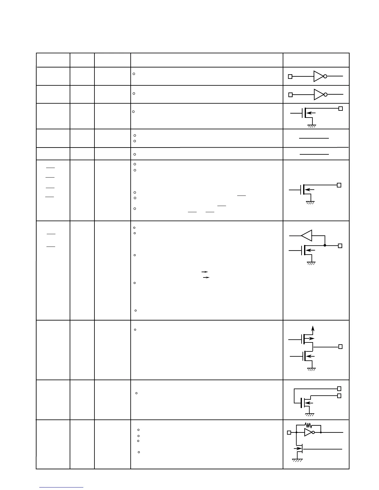
3.Pin function
Pin No.
19
VDD
Symbol
Functions
Type
Circut confguration
Ground
Dedicated output pins
The output states are determined by BO1 to BO4 in the
serial data.
'Data"=0:Open
=1:Low
The pins go to the open state after the power-on reset.
An 8Hz time base signal can be output from BO1 when TBC
in the serial data is set to 1.
Note that the ON impedance of the BO1 pin is higher than
that of the other pins (BO2 to BO4)
(2/2)
CL
4
Clock
Used as the synchronization clock when serial data is input
to the LC72131 (DI ), or when serial data is output (DO).
DI
3
Input data
Inputs serial data sent from the controller to the LC72131M.
DO
5
Output data
Output serial data sent from the LC72131M to the controller.
The content of the output data is determined by the serial
data DOCO to DOC2.
S
S
Output port
6
BO1
15
Power supply
The LC72131M power supply (VDD=4.5 to 5/5V)
The power on reset circuit operates when power is first applied.
VSS
The LC72131M ground.
BO2
BO3
BO4
7
8
9
12
11
17
18
16
IFIN
AIN
AOUT
Pins used for both input and output
The input or output state is determined by bits IOC1 and IOC2
in the serial state.
'Data"=0:Input port
=1:Output port
When specified for use as an input port :
The input state is transmitted to the controller through the
DO pin.
'Input state"=Low:data value 0
=High:data value 1
When specified for use as an output port :
The output state is determined by bits IO1 and IO2 in the
serial sate.
'Data"=0:Open
=1:Low
These pins go to the input port state after the power-on reset.
IF counter
The input frequency range is from 0.4 to 12MHz.
The signal is supplied directly to the IF counter.
The result from the IF counter MBS is output through
the DO pin.
There are four measurement periods: 4, 8, 32 or 64ms.
L.P.F
amplifier Tr
The MOS transistor used for the PLL active Low-pass filter.
PD
Charge pump
output
IO1
S
PLL Charge pump output
When the frequency generated by dividing the Local oscillator
frequency by N is higher than the reference frequency,
a high level will be output from the PD in. similarly, when that
frequency is lower, a low level will be output.
The PD pin goes to the high impedance state when the
frequencies agree.
10
IO2
I/O Port
 Loading...